OMRON CJ1W-MDAutomation Systems/ Programmable Controllers/CJ1
OMRON CJ1W-MD Automation Systems
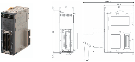
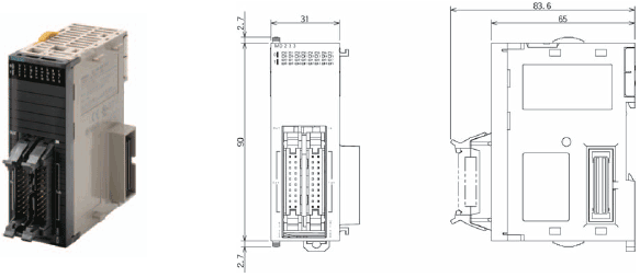
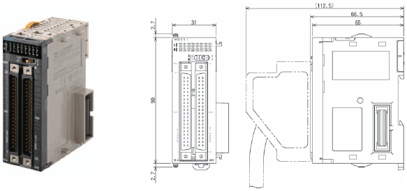
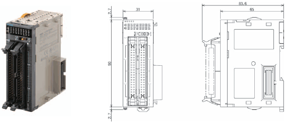
OMRON CJ1W-MD Dimensions
/Images/l_2056-25-118577-198x198.jpglast update: December 19, 2013
• Select the best interface for each application: Fujitsu connectors and MIL connectors.
• Select sinking outputs or sourcing outputs. The CJ1W-MD232 has load short-circuit protection.
• The ON and OFF response times can be set to between 0 and 32 ms in the Setup in the CPU Unit.
• Mixed I/O Units with 5-V TTL inputs are also available. *
• A wide variety of Connector-Terminal Block Conversion Units are available to allow you to easily wire external I/O devices.
* Applies to the CJ1W-MD563.
last update: December 19, 2013
Purchase the OMRON CJ1 Please fill in the following
If you have just landed here, this product OMRON CJ1W-MD Automation Systems,Automation Systems is offered online by Tianin FLD Technical Co.,Ltd. This is an online store providing Automation Systems at wholesale prices for consumers. You can call us or send enquiry, we would give you the prices, packing,deliverty and more detailed information on the CJ1W-MD We cooperate with DHL,TNT,FEDEX,UPS,EMS,etc.They guarantee to meet your needs in terms of time and money,even if you need your OMRON CJ1W-MDAutomation Systems tomorrow morning (aka overnight or next day air) on your desk, 2, 3 days or more.Note to international customers, YES, we ship worldwide.
WS02-SGWC1 / CPLC1 FA Communications Software/Features
A30NK Key-type Selector Switches/Features
E5ER-T Programmable Digital Controller/Features
CRT1-TS04T / TS04P Temperature Input Units/Features
K8DT-AW Single-phase Overcurrent/Undercurrent Relay/Features
OMRON CJ1W-MD dimension
CJ1W-MD CJ-series Mixed I/O Units/Dimensionslast update: December 19, 2013
32-point Units (Mixed I/O Units)
With Fujitsu-compatible connector (24-pin × 2)
CJ1W-MD231
With MIL connector (20-pin × 2)
CJ1W-MD232
CJ1W-MD233
64-point Units (Mixed I/O Units)
With Fujitsu-compatible connector (40-pin × 2)
CJ1W-MD261
With MIL connector (40-pin × 2)
CJ1W-MD263
CJ1W-MD563
last update: December 19, 2013
OMRON CJ1W-MD lineup
CJ1W-MD CJ-series Mixed I/O Units/Lineuplast update: May 7, 2018
International Standards
- The standards are abbreviated as follows: U: UL, U1: UL (Class I Division 2 Products for Hazardous Locations), C: CSA, UC: cULus, UC1: cULus (Class I Division 2 Products for Hazardous Locations), CU: cUL, N: NK, L: Lloyd, and CE: EC Directives.
- Contact your OMRON representative for further details and applicable conditions for these standards.
Mixed I/O Units
| Unit type | Product name | Specifications | Current con- sump- tion (A) | Model | Stand- ards | ||||||
|---|---|---|---|---|---|---|---|---|---|---|---|
| Output type | I/O points | Input voltage, Input current | Commons | Ex- ternal con- nec- tion | No. of words allo- cated | 5 V | 24 V | ||||
| Maximum switching capacity | |||||||||||
| CJ1 Basic I/O Units | DC Input/ Tran- sistor Output Units 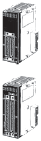 | Sinking | 16 inputs | 24 VDC, 7 mA | 16 points, 1 common | Fujitsu con- nector | 2 words | 0.13 | --- | CJ1W-MD231 | UC1, N, CE |
| 16 outputs | 250 VAC/ 24 VDC, 0.5 A | 16 points, 1 common | |||||||||
| Sinking | 16 inputs | 24 VDC, 7 mA | 16 points, 1 common | MIL con- nector | 2 words | 0.13 | --- | CJ1W-MD233 | UC1, N, CE | ||
| 16 outputs | 12 to 24 VDC, 0.5 A | 16 points, 1 common | |||||||||
| Sinking | 32 inputs | 24 VDC, 4.1 mA | 16 points, 1 common | Fujitsu con- nector | 4 words | 0.14 | --- | CJ1W-MD261 | |||
| 32 outputs | 12 to 24 VDC, 0.3 A | 16 points, 1 common | |||||||||
| Sinking | 32 inputs | 24 VDC, 4.1 mA | 16 points, 1 common | MIL con- nector | 4 words | 0.14 | --- | CJ1W-MD263 | |||
| 32 outputs | 12 to 24 VDC, 0.3 A | 16 points, 1 common | |||||||||
| Sourcing | 16 inputs | 24 VDC, 7 mA | 16 points, 1 common | MIL con- nector | 2 words | 0.13 | --- | CJ1W-MD232 | UC1, N, L, CE | ||
| 16 outputs | 24 VDC, 0.5 A Short- circuit protection | 16 points, 1 common | |||||||||
| TTL I/O Units  | --- | 32 inputs | 5 VDC, 35 mA | 16 points, 1 common | MIL con- nector | 4 words | 0.19 | --- | CJ1W-MD563 | UC1, N, CE | |
| 32 outputs | 5 VDC, 35 mA | 16 points, 1 common | |||||||||
Accessories
Connectors are not included for models with connectors. Either use one of the applicable connector listed below or use an applicable Connector-Terminal Block Conversion Unit or I/O Relay Terminal. For details on wiring methods, refer to External Interface.
Applicable Connectors
Fujitsu Connectors for 32-input, 32-output, 64-input, 64-output, 32-input/32-output, and 16-input/16-output Units
| Name | Con- nection | Remarks | Applicable Units | Model | Stand- ards | |
|---|---|---|---|---|---|---|
| 40-pin Con- nectors | Soldered | FCN-361J040-AU | Connector | Fujitsu Connectors: CJ1W-ID231(32 inputs): 1 per Unit CJ1W-ID261 (64 inputs): 2 per Unit CJ1W-OD231 (32 outputs): 1 per Unit CJ1W-OD261 (64 outputs): 2 per Unit CJ1W-MD261 (32 inputs, 32 outputs): 2 per Unit | C500-CE404 | --- |
| FCN-360C040-J2 | Connector Cover | |||||
| Crimped | FCN-363J040 | Housing | C500-CE405 | |||
| FCN-363J-AU | Contactor | |||||
| FCN-360C040-J2 | Connector Cover | |||||
| Pressure welded | FCN-367J040-AU/F | C500-CE403 | ||||
| 24-pin Con- nectors | Soldered | FCN-361J024-AU | Connector | Fujitsu Connectors: CJ1W-MD231 (16 inputs, 16 outputs): 2 per Unit | C500-CE241 | |
| FCN-360C024-J2 | Connector Cover | |||||
| Crimped | FCN-363J024 | Socket | C500-CE242 | |||
| FCN-363J-AU | Contactor | |||||
| FCN-360C024-J2 | Connector Cover | |||||
| Pressure welded | FCN-367J024-AU/F | C500-CE243 | ||||
MIL Connectors for 32-input, 32-output, 64-input, 64-output, 32-input/32-output, and 16-input/16-output Units
| Name | Con- nection | Remarks | Applicable Units | Model | Stand- ards |
|---|---|---|---|---|---|
| 40-pin Con- nectors | Pressure welded | FRC5-AO40-3TOS | MIL Connectors: CJ1W-ID232/233 (32 inputs): 1 per Unit CJ1W-OD232/233/234 (32 outputs):1 per Unit CJ1W-ID262 (64 inputs): 2 per Unit CJ1W-OD262/263 (64 outputs): 2 per Unit CJ1W-MD263/563 (32 inputs, 32 outputs): 2 per Unit | XG4M-4030-T | --- |
| Crimped | - | XG5N-401 * | |||
| 20-pin Con- nectors | Pressure welded | FRC5-AO20-3TOS | MIL Connectors: CJ1W-MD232/233 (16 inputs, 16 outputs): 2 per Unit | XG4M-2030-T | --- |
| Crimped | - | XG5N-201 * |
* Crimp Contacts are also required. Refer to Data Sheet for details.
Applicable Connector-Terminal Block Conversion Units
Size and Mounting are Refer to Data Sheet.
| Type/ Series | Num- ber of poles | Wiring method | Ter- minal type | Com- mon termi- nals | Bleeder resis- tance | Indi- cators | I/O Units | Model * | Stand- ards |
|---|---|---|---|---|---|---|---|---|---|
| General- purpose devices, PLC/ XW2R | 20 | Phillips screw  | M3 | No | No | No | CJ1W-MD231 CJ1W-MD232 CJ1W-MD233 | XW2R-J20GD-T | ― |
| 34 | CJ1W-MD261 | XW2R-J34GD-C1 | |||||||
| XW2R-J34GD-C3 | |||||||||
| CJ1W-MD263 | XW2R-J34GD-C2 | ||||||||
| XW2R-J34GD-C4 | |||||||||
| CJ1W-MD563 | XW2R-J34GD-C2 | ||||||||
| XW2R-J34GD-C4 | |||||||||
| 20 | Slotted screw (rise up)  | M3 (Euro- pean type) | CJ1W-MD231 CJ1W-MD232 CJ1W-MD233 | XW2R-E20GD-T | |||||
| 34 | CJ1W-MD261 | XW2R-E34GD-C1 | |||||||
| XW2R-E34GD-C3 | |||||||||
| CJ1W-MD263 | XW2R-E34GD-C2 | ||||||||
| XW2R-E34GD-C4 | |||||||||
| CJ1W-MD563 | XW2R-E34GD-C2 | ||||||||
| XW2R-E34GD-C4 | |||||||||
| 20 | Push-in spring  | Clamp | CJ1W-MD231 CJ1W-MD232 CJ1W-MD233 | XW2R-P20GD-T | |||||
| 34 | CJ1W-MD261 | XW2R-P34GD-C1 | |||||||
| XW2R-P34GD-C3 | |||||||||
| CJ1W-MD263 | XW2R-P34GD-C2 | ||||||||
| XW2R-P34GD-C4 | |||||||||
| CJ1W-MD563 | XW2R-P34GD-C2 | ||||||||
| XW2R-P34GD-C4 |
Note: For the combination of Input Units with Connector-Terminal Block Conversion Units, refer to 2. Connecting
Connector-Terminal Block Conversion Units.
* Representative models only. For details, refer to the XW2R series catalog (Cat. No. G077).
Connecting Cables for Connector-Terminal Block Conversion Units
| Appearance | Connectors | Cable lenght [m] | Model |
|---|---|---|---|
XW2Z-[][][]A | One 24-pin Fujitsu Connector to One 20-pin MIL Connector | 0.5 | XW2Z-050A |
| 1 | XW2Z-100A | ||
| 1.5 | XW2Z-150A | ||
| 2 | XW2Z-200A | ||
| 3 | XW2Z-300A | ||
| 5 | XW2Z-500A | ||
| 7 | XW2Z-700A | ||
| 10 | XW2Z-010A | ||
| 15 | XW2Z-15MA | ||
| 20 | XW2Z-20MA | ||
XW2Z-[][][]X | One 20-pin MIL Connector to One 20-pin MIL Connector | 0.5 | XW2Z-C50X |
| 1 | XW2Z-100X | ||
| 2 | XW2Z-200X | ||
| 3 | XW2Z-300X | ||
| 5 | XW2Z-500X | ||
| 10 | XW2Z-010X | ||
XW2Z-[][][]PF | One 40-pin Fujitsu Connector to One 40-pin MIL Connector | 0.5 | XW2Z-050PF |
| 1 | XW2Z-100PF | ||
| 1.5 | XW2Z-150PF | ||
| 2 | XW2Z-200PF | ||
| 3 | XW2Z-300PF | ||
| 5 | XW2Z-500PF | ||
XW2Z-[][][]PM | One 40-pin MIL Connector to One 40-pin MIL Connector | 0.5 | XW2Z-050PM |
| 1 | XW2Z-100PM | ||
| 1.5 | XW2Z-150PM | ||
| 2 | XW2Z-200PM | ||
| 3 | XW2Z-300PM | ||
| 5 | XW2Z-500PM |
Applicable I/O Relay Terminals
Size (horizontal mounting) and Mounting are Refer to Data Sheet.
| Type/ Series | Specifications | Model | Stand- ards | |||||
|---|---|---|---|---|---|---|---|---|
| Classifi- cation | Po- lar- ity | Number of points | Rated ON cur- rent at con- tacts | Rated vol- tage | ||||
| Push-In Plus terminal block/ G70V | In- puts | DC inputs | NPN | 16 (SPST- NO × 16) | 50 mA | 24 VDC | G70V-SID16P *4 | UC, CE (TÜV certi- fied) |
| PNP | G70V-SID16P-1 *4 | |||||||
| NPN | G70V-SID16P-C16 *5 | |||||||
| PNP | G70V-SID16P-1-C16 *5 | |||||||
| Out- puts | Relay outputs | NPN | 16 (SPDT × 16) | 6 A/ point, 10 A/ common | G70V-SOC16P *4 | |||
| PNP | G70V-SOC16P-1 *4 | |||||||
| NPN | G70V-SOC16P-C4 *6 | |||||||
| PNP | G70V-SOC16P-1-C4 *6 | |||||||
| Standard/ G7TC | In- puts | AC inputs | NPN | 16 (SPST- NO × 16) | 1A | 100/(110) VAC | G7TC-IA16 AC100/110 | U, C |
| 200/(220) VAC | G7TC-IA16 AC200/220 | |||||||
| DC inputs | 12 VDC | G7TC-ID16 DC12 | ||||||
| 24 VDC | G7TC-ID16 DC24 | |||||||
| 100/110 VDC | G7TC-ID16 DC100/110 | |||||||
| Out- puts | Relay outputs | NPN | 8 (SPST- NO × 8) | 5A | 12 VDC | G7TC-OC08 DC12 | ||
| 24 VDC | G7TC-OC08 DC24 | |||||||
| 16 (SPST- NO × 16) | 12 VDC | G7TC-OC16 DC12 | ||||||
| 24 VDC | G7TC-OC16 DC24 | |||||||
| PNP | 16 (SPST- NO × 16) | 12 VDC | G7TC-OC16-1 DC12 | |||||
| 24 VDC | G7TC-OC16-1 DC24 | |||||||
| High- capacity socket/ G70A *1 (Socket only) | In- puts | Relay inputs | NPN/ PNP | 16 (SPDT × 16 possible with G2R Relays) | 100 mA | 110 VDC max., 240 VAC max. *2 | G70A-ZOC16-5 | U, C, CE (VDE certi- fied) |
| Out- puts | Relay outputs | NPN | 10 A (Terminal block allowable | 24 VDC | G70A-ZOC16-3 | |||
| PNP | G70A-ZOC16-4 | |||||||
| Space- saving/ Vertical type G70D-V | Out- puts | Relay outputs | NPN | 16 (SPST- NO × 16) | 5 A or 3 A *3 | 24 VDC | G70D-VSOC16 | U, C, CE (VDE certi- fied) |
| MOSFET relay outputs | 0.3 A | G70D-VFOM16 | ||||||
| Space- saving/ Flat type G70D | Relay outputs | NPN | 8 (SPST- NO × 8) | 5 A | G70D-SOC08 | - | ||
| 16 (SPST- NO × 16) | 3 A | G70D-SOC16 | ||||||
| PNP | 16 (SPST- NO × 16) | 3 A | G70D-SOC16-1 | |||||
| MOSFET relay outputs | NPN | 16 (SPST- NO × 16) | 0.3 A | G70D-FOM16 | ||||
| PNP | G70D-FOM16-1 | |||||||
| High- ca- pacity, space- saving/ G70R | Out- puts | Relay outputs | NPN | 8 (SPST- NO × 8) | 10 A | 24 VDC | G70R-SOC08 | - |
*1. G70A is a I/O terminal socket product. Relay is not provided with the socket. Be sure to order a relay, timer separately.
*2. Each relay to be mounted must incorporate a coil that has proper specifications within the maximum rated voltage range.
*3. Eight or fewer points ON: 5 A, Nine or more points ON: 3 A.
*4. Internal common at terminal block: No internal connections
*5. Internal common at terminal block: Internal IO common 16 points internally connected
*6. Internal common at terminal block: Every 4 points internally connected at terminal block middle row.
Note: 1. For the combination of Input Units with I/O Relay Terminal and Connecting Cables, refer to 3. Connecting I/O
Relay Terminals.
2. Please refer to each Datasheet about details.
3. When the G7TC is used with an AC rated voltage, three rated currents can be used.
If a coil voltage of 110 or 220 VAC is used, 50 Hz cannot be used.
Cables for I/O Relay Terminals
| Type | Name | I/O Classifi- cation | Appearance | Cable length L (mm) | Models |
|---|---|---|---|---|---|
| Fujitsu connectors (24 pins) | Cables with Connectors (1:1) XW2Z-R[]C | 16 I/O points |  | 1,000 | XW2Z-R100C |
| 1,500 | XW2Z-R150C | ||||
| 2,000 | XW2Z-R200C | ||||
| 3,000 | XW2Z-R300C | ||||
| 5,000 | XW2Z-R500C | ||||
| Fujitsu connectors (40 pins) | Cables with Connectors (1:2) XW2Z-RI[]C-[] XW2Z-RO[]C-[] | 32 input points |  | (A) 1,000 (B) 750 | XW2Z-RI100C-75 |
| (A) 1,500 (B) 1,250 | XW2Z-RI150C-125 | ||||
| (A) 2,000 (B) 1,750 | XW2Z-RI200C-175 | ||||
| (A) 3,000 (B) 2,750 | XW2Z-RI300C-275 | ||||
| (A) 5,000 (B) 4,750 | XW2Z-RI500C-475 | ||||
| 32 output points | (A) 1,000 (B) 750 | XW2Z-RO100C-75 | |||
| (A) 1,500 (B) 1,250 | XW2Z-RO150C-125 | ||||
| (A) 2,000 (B) 1,750 | XW2Z-RO200C-175 | ||||
| (A) 3,000 (B) 2,750 | XW2Z-RO300C-275 | ||||
| (A) 5,000 (B) 4,750 | XW2Z-RO500C-475 | ||||
| MIL connectors (20 pins) | Cables with Connectors (1:1) XW2Z-RI[]C XW2Z-RO[]C | 16 I/O points |  | 250 | XW2Z-RI25C |
| 500 | XW2Z-RI50C | ||||
| 250 | XW2Z-RO25C | ||||
| 500 | XW2Z-RO50C | ||||
| MIL connectors (40 pins) | Cables with Connectors (1:2) XW2Z-RO[]-[]-D1, XW2Z-RI[]-[]-D1 | 32 I/O points |  | (A) 500 (B) 250 | XW2Z-RO50-25-D1 |
| (A) 750 (B) 500 | XW2Z-RO75-50-D1 | ||||
| (A) 1,000 (B) 750 | XW2Z-RO100-75-D1 | ||||
| (A) 1,500 (B) 1,250 | XW2Z-RO150-125-D1 | ||||
| (A) 2,000 (B) 1,750 | XW2Z-RO200-175-D1 | ||||
| (A) 3,000 (B) 2,750 | XW2Z-RO300-275-D1 | ||||
| (A) 5,000 (B) 4,750 | XW2Z-RO500-475-D1 | ||||
| (A) 500 (B) 250 | XW2Z-RI50-25-D1 | ||||
| (A) 750 (B) 500 | XW2Z-RI75-50-D1 | ||||
| (A) 1,000 (B) 750 | XW2Z-RI100-75-D1 | ||||
| (A) 1,500 (B) 1,250 | XW2Z-RI150-125-D1 | ||||
| (A) 2,000 (B) 1,750 | XW2Z-RI200-175-D1 | ||||
| (A) 3,000 (B) 2,750 | XW2Z-RI300-275-D1 | ||||
| (A) 5,000 (B) 4,750 | XW2Z-RI500-475-D1 |
Note: Refer to the Datasheet for the XW2Z-R Cables for I/O Relay Terminals (Cat. No. G126).
last update: May 7, 2018
OMRON CJ1W-MD catalog
CJ1W-MD CJ-series Mixed I/O Units/Catalog- Catalog
- Manual
- CAD
English
Global Edition
| Catalog Name | Catalog Number [size] | Last Update | |
|---|---|---|---|
| | - [3193KB] | May 07, 201820180507 | CJ1W-MD Data Sheet |
| | G126-E1-02 [2435KB] | Apr 03, 201720170403 | XW2Z-R Data Sheet |
| | J217-E1-02 [1206KB] | Jun 01, 201820180601 | G70[]/G7TC Table of I/O Relay Terminal and connectable device combinations |
| | G129-E1-02 [950KB] | Jun 01, 201820180601 | XW2 Series Table of Connector-Terminal Block Conversion Units and connectable device combinations |
OMRON CJ1W-MD specification
CJ1W-MD CJ-series Mixed I/O Units/Specificationslast update: July 06, 2016
CJ1W-MD231 DC Input/Transistor Output Unit (24 VDC, 16 Inputs/16 Outputs)
| Name | 16-point DC Input/16-point Transistor Output Unit with Fujitsu Connectors (Sinking Outputs) | ||
|---|---|---|---|
| Model | CJ1W-MD231 | ||
| Output section (CN1) | Input section (CN2) | ||
| Rated Voltage | 12 to 24 VDC | Rated Input Voltage | 24 VDC |
| Operating Load Voltage Range | 10.2 to 26.4 VDC | Operating Input Voltage | 20.4 to 26.4 VDC |
| Maximum Load Current | 0.5 A/point, 2.0 A/Unit | Input Impedance | 3.3 kΩ |
| Maximum Inrush Current | 4.0 A/point, 10 ms max. | Input Current | 7 mA typical (at 24 VDC) |
| Leakage Current | 0.1 mA max. | ON Voltage/ON Current | 14.4 VDC min./3 mA min. |
| Residual Voltage | 1.5 V max. | OFF Voltage/OFF Current | 5 VDC max./1 mA max. |
| ON Response Time | 0.1 ms max. | ON Response Time | 8.0 ms max. (Can be set to between 0 and 32 in the Setup.) * |
| OFF Response Time | 0.8 ms max. | ||
| No. of Circuits | 16 (16 points/common, 1 circuit) | OFF Response Time | 8.0 ms max. (Can be set to between 0 and 32 in the Setup.) * |
| Fuse | None | ||
| External Power Supply | 10.2 to 26.4 VDC, 20 mA min. | No. of Circuits | 16 (16 points/common, 1 circuit) |
| Number of Simultaneously ON Points | 75% (at 24 VDC) | ||
| Insulation Resistance | 20 MΩ min. between the external terminals and the GR terminal (at 100 VDC) | ||
| Dielectric Strength | 1,000 VAC between the external terminals and the GR terminal for 1 minute at a leakage current of 10 mA max. | ||
| Internal Current Consumption | 5 VDC 130 mA max. | ||
| Weight | 90 g max. | ||
| Accessories | None | ||
| Circuit Configuration | CN1 (OUT) | CN2 (IN) | |
 The signal names of the terminals are the The signal names of the terminals are thedevice variable names. The device variable names are the names that use "Jxx" as the device name. |   The signal names of the terminals are the The signal names of the terminals are thedevice variable names. The device variable names are the names that use "Jxx" as the device name. | ||
| External connection and terminal-device variable diagram | CN1 (OUT) | CN2 (IN) | |
 When wiring, pay careful attention to the polarity When wiring, pay careful attention to the polarityof the external power supply. The load may operate incorrectly if polarity is reversed. Be sure to wire both pins A9 and B9 (COM0 (0 V)) of CN1. Be sure to wire both pins A10 and B10 (+V) of CN1. The signal names of the terminals are the device variable names. The device variable names are the names that use "Jxx" as the device name. |  When wiring, pay careful attention to the polarity When wiring, pay careful attention to the polarityof the external power supply. The load may operate incorrectly if polarity is reversed. Be sure to wire both pins A9 and B9 (COM1) of CN2, and set the same polarity for both pins. The signal names of the terminals are the device variable names. The device variable names are the names that use "Jxx" as the device name. | ||
* The ON response time will be 20 μs maximum and OFF response time will be 400 μs maximum even if the response
times are set to 0 ms due to internal element delays.
CJ1W-MD233 DC Input/Transistor Output Unit (24 VDC, 16 Inputs/16 Outputs)
| Name | 16-point DC Input/16-point Transistor Output Unit with MIL Connectors (Sinking Outputs) | ||
|---|---|---|---|
| Model | CJ1W-MD233 | ||
| Output section (CN1) | Input section (CN2) | ||
| Rated Voltage | 12 to 24 VDC | Rated Input Voltage | 24 VDC |
| Operating Load Voltage Range | 10.2 to 26.4 VDC | Operating Input Voltage | 20.4 to 26.4 VDC |
| Maximum Load Current | 0.5 A/point, 2.0 A/Unit | Input Impedance | 3.3 kΩ |
| Maximum Inrush Current | 4.0 A/point, 10 ms max. | Input Current | 7 mA typical (at 24 VDC) |
| Leakage Current | 0.1 mA max. | ON Voltage/ON Current | 14.4 VDC min./3 mA min. |
| Residual Voltage | 1.5 V max. | OFF Voltage/OFF Current | 5 VDC max./1 mA max. |
| ON Response Time | 0.1 ms max. | ON Response Time | 8.0 ms max. (Can be set to between 0 and 32 in the Setup.) * |
| OFF Response Time | 0.8 ms max. | ||
| No. of Circuits | 16 (16 points/common, 1 circuit) | OFF Response Time | 8.0 ms max. (Can be set to between 0 and 32 in the Setup.) * |
| Fuse | None | ||
| External Power Supply | 10.2 to 26.4 VDC, 20 mA min. | No. of Circuits | 16 (16 points/common, 1 circuit) |
| Number of Simultaneously ON Points | 75% (at 24 VDC) | ||
| Insulation Resistance | 20 MΩ min. between the external terminals and the GR terminal (at 100 VDC) | ||
| Dielectric Strength | 1,000 VAC between the external terminals and the GR terminal for 1 minute at a leakage current of 10 mA max. | ||
| Internal Current Consumption | 5 VDC 130 mA max. | ||
| Weight | 90 g max. | ||
| Accessories | None | ||
| Circuit Configuration | CN1 (OUT) | CN2 (IN) | |
 The signal names of the terminals are the The signal names of the terminals are thedevice variable names. The device variable names are the names that use "Jxx" as the device name. |   The signal names of the terminals are the The signal names of the terminals are thedevice variable names. The device variable names are the names that use "Jxx" as the device name. | ||
| External connection and terminal-device variable diagram | CN1 (OUT) | CN2 (IN) | |
 When wiring, pay careful attention to the polarity When wiring, pay careful attention to the polarityof the external power supply. The load may operate incorrectly if polarity is reversed. Be sure to wire both terminals 3 and 4 (COM0 (0 V)) of CN1. Be sure to wire both terminals 1 and 2 (+V) of CN1. The signal names of the terminals are the device variable names. The device variable names are the names that use "Jxx" as the device name. |  When wiring, pay careful attention to the polarity When wiring, pay careful attention to the polarityof the external power supply. The load may operate incorrectly if polarity is reversed. Be sure to wire both pins 3 and 4 (COM1) of CN2, and set the same polarity for both pins. The signal names of the terminals are the device variable names. The device variable names are the names that use "Jxx" as the device name. | ||
* The ON response time will be 20 μs maximum and OFF response time will be 400 μs maximum even if the response
times are set to 0 ms due to internal element delays.
CJ1W-MD261 DC Input/Transistor Output Unit (24 VDC 32 Inputs/32 Outputs)
| Name | 32-point DC Input/32-point Transistor Output Unit with Fujitsu Connectors (Sinking Outputs) | ||
|---|---|---|---|
| Model | CJ1W-MD261 | ||
| Output section (CN1) | Input section (CN2) | ||
| Rated Voltage | 12 to 24 VDC | Rated Input Voltage | 24 VDC |
| Operating Load Voltage Range | 10.2 to 26.4 VDC | Operating Input Voltage | 20.4 to 26.4 VDC |
| Maximum Load Current | 0.3 A/point, 1.6 A/common, 3.2 A/Unit | Input Impedance | 5.6 kΩ |
| Maximum Inrush Current | 3.0 A/point, 10 ms max. | Input Current | 4.1 mA typical (at 24 VDC) |
| Leakage Current | 0.1 mA max. | ON Voltage/ON Current | 19.0 VDC min./3 mA min. *2 |
| Residual Voltage | 1.5 V max. | OFF Voltage/OFF Current | 5 VDC max./1 mA max. |
| ON Response Time | 0.5 ms max. | ON Response Time | 8.0 ms max. (Can be set to between 0 and 32 in the Setup.) *1 |
| OFF Response Time | 1.0 ms max. | ||
| No. of Circuits | 32 (16 points/common, 2 circuits) | OFF Response Time | 8.0 ms max. (Can be set to between 0 and 32 in the Setup.) *1 |
| Fuse | None | ||
| External Power Supply | 10.2 to 26.4 VDC, 30 mA min. | No. of Circuits | 32 (16 points/common, 2 circuits) |
| Number of Simultaneously ON Points | 75% (24 points) (at 24 VDC) | ||
| Insulation Resistance | 20 MΩ min. between the external terminals and the GR terminal (at 100 VDC) | ||
| Dielectric Strength | 1,000 VAC between the external terminals and the GR terminal for 1 minute at a leakage current of 10 mA max. | ||
| Internal Current Consumption | 5 VDC 140 mA max. | ||
| Weight | 110 g max. | ||
| Accessories | None | ||
| Circuit Configuration | CN1 (OUT) | CN2 (IN) | |
 The signal names of the terminals are the The signal names of the terminals are thedevice variable names. The device variable names are the names that use "Jxx" as the device name. |  The signal names of the terminals are the The signal names of the terminals are thedevice variable names. The device variable names are the names that use "Jxx" as the device name. | ||
 | |||
| External connection and terminal-device variable diagram | CN1 (OUT) | CN2 (IN) | |
 Be sure to wire both terminals A19 and A9 Be sure to wire both terminals A19 and A9(COM0 (0 V)) of CN1. Be sure to wire both terminals B19 and B9 (COM1 (0 V)) of CN1. Be sure to wire both terminals A20 and A10 (+V) of CN1. Be sure to wire both terminals B20 and B10 (+V) of CN1. When wiring, pay careful attention to the polarity of the external power supply. The load may operate incorrectly if polarity is reversed. The signal names of the terminals are the device variable names. The device variable names are the names that use "Jxx" as the device name. |  Be sure to wire both pins A9 and A18 (COM2) of Be sure to wire both pins A9 and A18 (COM2) ofCN2, and set the same polarity for both pins. Be sure to wire both pins B9 and B18 (COM3) of CN2, and set the same polarity for both pins. When wiring, pay careful attention to the polarity of the external power supply. The load may operate incorrectly if polarity is reversed. The signal names of the terminals are the device variable names. The device variable names are the names that use "Jxx" as the device name. | ||
*1. The ON response time will be 120 μs maximum and OFF response time will be 400 μs maximum even if the
response times are set to 0 ms due to internal element delays.
*2. Observe the following restrictions when connecting to a 2-wire sensor.
• Make sure the input power supply voltage is larger than the ON voltage (19 V) plus the residual voltage of the
sensor (approx. 3 V).
• Use a sensor with a minimum load current of 3 mA min.
• Connect bleeder resistance if you connect a sensor with a minimum load current of 5 mA or higher.
CJ1W-MD263 DC Input/Transistor Output Unit (24 VDC 32 Inputs/32 Outputs)
| Name | 32-point DC Input/32-point Transistor Output Unit with MIL Connectors (Sinking Outputs) | ||
|---|---|---|---|
| Model | CJ1W-MD263 | ||
| Output section (CN1) | Input section (CN2) | ||
| Rated Voltage | 12 to 24 VDC | Rated Input Voltage | 24 VDC |
| Operating Load Voltage Range | 10.2 to 26.4 VDC | Operating Input Voltage | 20.4 to 26.4 VDC |
| Maximum Load Current | 0.3 A/point, 1.6 A/common, 3.2 A/Unit | Input Impedance | 5.6 kΩ |
| Maximum Inrush Current | 3.0 A/point, 10 ms max. | Input Current | 4.1 mA typical (at 24 VDC) |
| Leakage Current | 0.1 mA max. | ON Voltage/ON Current | 19.0 VDC min./3 mA min. *2 |
| Residual Voltage | 1.5 V max. | OFF Voltage/OFF Current | 5 VDC max./1 mA max. |
| ON Response Time | 0.5 ms max. | ON Response Time | 8.0 ms max. (Can be set to between 0 and 32 in the Setup.) *1 |
| OFF Response Time | 1.0 ms max. | ||
| No. of Circuits | 32 (16 points/common, 2 circuits) | OFF Response Time | 8.0 ms max. (Can be set to between 0 and 32 in the Setup.) *1 |
| Fuse | None | ||
| External Power Supply | 10.2 to 26.4 VDC, 30 mA min. | No. of Circuits | 32 (16 points/common, 2 circuits) |
| Number of Simultaneously ON Points | 75% (24 points) (at 24 VDC) | ||
| Insulation Resistance | 20 MΩ min. between the external terminals and the GR terminal (at 100 VDC) | ||
| Dielectric Strength | 1,000 VAC between the external terminals and the GR terminal for 1 minute at a leakage current of 10 mA max. | ||
| Internal Current Consumption | 5 VDC 140 mA max. | ||
| Weight | 110 g max. | ||
| Accessories | None | ||
| Circuit Configuration | CN1 (OUT) | CN2 (IN) | |
 The signal names of the terminals are the The signal names of the terminals are thedevice variable names. The device variable names are the names that use "Jxx" as the device name. |  The signal names of the terminals are the The signal names of the terminals are thedevice variable names. The device variable names are the names that use "Jxx" as the device name. | ||
 | |||
| External connection and terminal-device variable diagram | CN1 (OUT) | CN2 (IN) | |
 Be sure to wire both terminals 23 and 24 Be sure to wire both terminals 23 and 24(COM0) of CN1. Be sure to wire both terminals 3 and 4 (COM1) of CN1. Be sure to wire both terminals 21 and 22 (+V) of CN1. Be sure to wire both terminals 1 and 2 (+V) of CN1. When wiring, pay careful attention to the polarity of the external power supply. The load may operate incorrectly if polarity is reversed. The signal names of the terminals are the device variable names. The device variable names are the names that use "Jxx" as the device name. |  Be sure to wire both pins 23 and 24 (COM2) of Be sure to wire both pins 23 and 24 (COM2) ofCN2, and set the same polarity for both pins. Be sure to wire both pins 3 and 4 (COM3) of CN2, and set the same polarity for both pins. When wiring, pay careful attention to the polarity of the external power supply. The load may operate incorrectly if polarity is reversed. The signal names of the terminals are the device variable names. The device variable names are the names that use "Jxx" as the device name. | ||
*1. The ON response time will be 120 μs maximum and OFF response time will be 400 μs maximum even if the
response times are set to 0 ms due to internal element delays.
*2. Observe the following restrictions when connecting to a 2-wire sensor.
• Make sure the input power supply voltage is larger than the ON voltage (19 V) plus the residual voltage of the
sensor (approx. 3 V).
• Use a sensor with a minimum load current of 3 mA min.
• Connect bleeder resistance if you connect a sensor with a minimum load current of 5 mA or higher.
CJ1W-MD232 DC Input/Transistor Output Unit (24 VDC, 16 inputs/16 Outputs)
| Name | 16-point DC Input/16-point Transistor Output Unit with MIL Connectors (Sourcing Outputs) | ||
|---|---|---|---|
| Model | CJ1W-MD232 | ||
| Output section (CN1) | Input section (CN2) | ||
| Rated Voltage | 24 VDC | Rated Input Voltage | 24 VDC |
| Operating Load Voltage Range | 20.4 to 26.4 VDC | Operating Input Voltage | 20.4 to 26.4 VDC |
| Maximum Load Current | 0.5 A/point, 2.0 A/Unit | Input Impedance | 3.3 kΩ |
| Leakage Current | 0.1 mA max. | Input Current | 7 mA typical (at 24 VDC) |
| Residual Voltage | 1.5 V max. | ON Voltage/ON Current | 14.4 VDC min./3 mA min. |
| ON Response Time | 0.5 ms max. | OFF Voltage/OFF Current | 5 VDC max./1 mA max. |
| OFF Response Time | 1.0 ms max. | ON Response Time | 8.0 ms max. (Can be set to between 0 and 32 in the Setup.) * |
| Load Short- circuit Protection | Detection current: 0.7 to 2.5 A min. Automatic restart after error clearance. | OFF Response Time | 8.0 ms max. (Can be set to between 0 and 32 in the Setup.) * |
| No. of Circuits | 16 (16 points/common, 1 circuit) | No. of Circuits | 16 (16 points/common, 1 circuit) |
| External Power Supply | 20.4 to 26.4 VDC, 40 mA min. | Number of Simultaneously ON Points | 75% (at 24 VDC) |
| Insulation Resistance | 20 MΩ min. between the external terminals and the GR terminal (at 100 VDC) | ||
| Dielectric Strength | 1,000 VAC between the external terminals and the GR terminal for 1 minute at a leakage current of 10 mA max. | ||
| Internal Current Consumption | 5 VDC 130 mA max. | ||
| Weight | 100 g max. | ||
| Accessories | None | ||
| Circuit Configuration | CN1 (OUT) | CN2 (IN) | |
 The signal names of the terminals are the The signal names of the terminals are thedevice variable names. The device variable names are the names that use "Jxx" as the device name. |  The signal names of the terminals are the The signal names of the terminals are thedevice variable names. The device variable names are the names that use "Jxx" as the device name. | ||
 | |||
| External connection and terminal-device variable diagram | CN1 (OUT) | CN2 (IN) | |
 When wiring, pay careful attention to the polarity When wiring, pay careful attention to the polarityof the external power supply. The load may operate incorrectly if polarity is reversed. Be sure to wire both terminals 3 and 4 (COM0 (+V)) of CN1. Be sure to wire both terminals 1 and 2 (0 V) of CN1. The signal names of the terminals are the device variable names. The device variable names are the names that use "Jxx" as the device name. |  When wiring, pay careful attention to the polarity When wiring, pay careful attention to the polarityof the external power supply. The load may operate incorrectly if polarity is reversed. Be sure to wire both pins 3 and 4 (COM1) of CN2, and set the same polarity for both pins. The signal names of the terminals are the device variable names. The device variable names are the names that use "Jxx" as the device name. | ||
* The ON response time will be 20 μs maximum and OFF response time will be 400 μs maximum even if the response
times are set to 0 ms due to internal element delays.
CJ1W-MD563 TTL I/O Unit (32 Inputs/32 Outputs)
| Name | 32-point Input /32-point Output TTL I/O Unit with MIL Connectors | ||
|---|---|---|---|
| Model | CJ1W-MD563 | ||
| Output section (CN1) | Input section (CN2) | ||
| Rated Voltage | 5 VDC±10% | Rated Input Voltage | 5 VDC±10% |
| Operating Load Voltage Range | 4.5 to 5.5 VDC | Input Impedance | 1.1 kΩ |
| Maximum Load Current | 35 mA/point, 560 mA/common, 1.12 A/Unit | Input Current | Approx. 3.5 mA (at 5 VDC) |
| Leakage Current | 0.1 mA max. | ON Voltage | 3.0 VDC min. |
| Residual Voltage | 0.4 V max. | OFF Voltage | 1.0 VDC max. |
| ON Response Time | 0.2 ms max. | ON Response Time | 8.0 ms max. (Can be set to between 0 and 32 in the Setup.) * |
| OFF Response Time | 0.3 ms max. | OFF Response Time | 8.0 ms max. (Can be set to between 0 and 32 in the Setup.) * |
| No. of Circuits | 32 points (16 points/common, 2 circuits) | ||
| Fuse | None | No. of Circuits | 32 points (16 points/ common, 2 circuits) |
| External Power Supply | 5 VDC ± 10%, 40 mA min. (1.2 mA × No. of ON points) | Number of Simultaneously ON Points | 100% (16 points/ common) |
| Insulation Resistance | 20 MΩ min. between the external terminals and the GR terminal (at 100 VDC) | ||
| Dielectric Strength | 1,000 VAC between the external terminals and the GR terminal for 1 minute at a leakage current of 10 mA max. | ||
| Internal Current Consumption | 5 VDC 190 mA max. | ||
| Weight | 110 g max. | ||
| Accessories | None | ||
| Circuit Configuration | CN1 (OUT) | CN2 (IN) | |
 The signal names of the terminals are the The signal names of the terminals are thedevice variable names. The device variable names are the names that use "Jxx" as the device name. |  The signal names of the terminals are the The signal names of the terminals are thedevice variable names. The device variable names are the names that use "Jxx" as the device name. | ||
| External connection and terminal-device variable diagram | CN1 (OUT) | CN2 (IN) | |
 When wiring, pay careful attention to the polarity When wiring, pay careful attention to the polarityof the external power supply. The load may operate incorrectly if the polarity is reversed. Be sure to wire both terminals 23 and 24 (COM0) of CN1. Be sure to wire both terminals 3 and 4 (COM1) of CN1. Be sure to wire both terminals 21 and 22 (+V) of CN1. Be sure to wire both terminals 1 and 2 (+V) of CN1. The signal names of the terminals are the device variable names. The device variable names are the names that use "Jxx" as the device name. |  When wiring, pay careful attention to the polarity When wiring, pay careful attention to the polarityof the external power supply. The load may operate incorrectly if the polarity is reversed. Be sure to wire both pins 23 and 24 (COM2) of CN2, and set the same polarity for both pins. Be sure to wire both pins 3 and 4 (COM3) of CN2, and set the same polarity for both pins. The signal names of the terminals are the device variable names. The device variable names are the names that use "Jxx" as the device name. | ||
* The ON response time will be 120 μs maximum and OFF response time will be 400 μs maximum even if the response
times are set to 0 ms due to internal element delays.
Bit Allocations for Mixed I/O Unit
32-point Mixed I/O Unit
| Allocated CIO word | Signal name ( | |
| CIO | Bit | |
| Wd m ( | 00 | OUT0/ |
| 01 | OUT1/ | |
| : | : | |
| 14 | OUT14/ | |
| 15 | OUT15/ | |
| Wd m+ ( | 00 | IN0/ |
| 01 | IN1/ | |
| : | : | |
| 14 | IN14/ | |
| 15 | IN15/ | |
32-point Mixed I/O Unit
| Allocated CIO word | Signal name ( | |
| CIO | Bit | |
| Wd m ( | 00 | OUT0/ |
| 01 | OUT1/ | |
| : | : | |
| 14 | OUT14/ | |
| 15 | OUT15/ | |
| Wd m+ ( | 00 | OUT0/ |
| 01 | OUT1/ | |
| : | : | |
| 14 | OUT14/ | |
| 15 | OUT15/ | |
| Wd m+ ( | 00 | IN0/ |
| 01 | IN1/ | |
| : | : | |
| 14 | IN14/ | |
| 15 | IN15/ | |
| Wd m+ ( | 00 | IN0/ |
| 01 | IN1/ | |
| : | : | |
| 14 | IN14/ | |
| 15 | IN15/ | |
last update: July 06, 2016
- NO. CJ1W-MD
- TYPE:Programmable Controllers CJ1 Basic I/O Units
- DATE:2021-06-12
- Associated products:
CJ1W-OC / OA / OD CJ-series Output Units/Features CJ1W-INT01 CJ-series Interrupt Input Units/Features