OMRON CJ1W-OC / OA / ODAutomation Systems/ Programmable Controllers/CJ1
OMRON CJ1W-OC / OA / OD Automation Systems
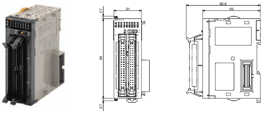
OMRON CJ1W-OC / OA / OD Dimensions
/Images/l_2055-25-118582-198x198.jpglast update: December 19, 2013
• High-speed output models are available, meeting versatile applications.
ON Response Time: 15μs, OFF Response Time: 80μs
• Output Units are available with any of three output types: relay contact outputs, triac outputs, or transistor outputs.
• For transistor outputs, select from sinking outputs or sourcing outputs.
• Output Units with load short-circuit protection are also available. *1
• Select the best interface for each application: Fujitsu connectors or MIL connectors. *2
• A wide variety of Connector-Terminal Block Conversion Units are available to allow you to easily wire external output devices.
*1. The following Units have load short-circuit protection: CJ1W-OC202, CJ1W-OD204, CJ1W-OD212, and CJ1W-OD232.
*2. Available for models with 32 outputs or 64 outputs
last update: December 19, 2013
Purchase the OMRON CJ1 Please fill in the following
If you have just landed here, this product OMRON CJ1W-OC / OA / OD Automation Systems,Automation Systems is offered online by Tianin FLD Technical Co.,Ltd. This is an online store providing Automation Systems at wholesale prices for consumers. You can call us or send enquiry, we would give you the prices, packing,deliverty and more detailed information on the CJ1W-OC / OA / OD We cooperate with DHL,TNT,FEDEX,UPS,EMS,etc.They guarantee to meet your needs in terms of time and money,even if you need your OMRON CJ1W-OC / OA / ODAutomation Systems tomorrow morning (aka overnight or next day air) on your desk, 2, 3 days or more.Note to international customers, YES, we ship worldwide.
E3ZM-V Color Mark Detection Compact Photoelectric Sensor/Features
ZW Series Confocal Fiber Displacement Sensor/Features
E2EQ Spatter-resistant Proximity Sensor/Features
NSJ Series Programmable Controllers/Features
GRT1-DRT DeviceNet Communications Unit/Features
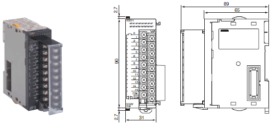
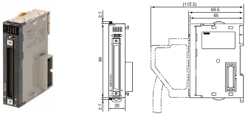
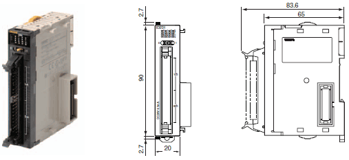
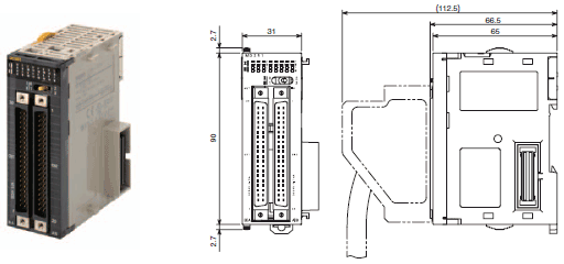
OMRON CJ1W-OC / OA / OD dimension
CJ1W-OC / OA / OD CJ-series Output Units/Dimensionslast update: December 19, 2013
8-point/16-point Units (18-point Terminal Blocks)
CJ1W-OC201/OC211/OA201/OD201/OD202/OD203/OD204/OD211/OD213 /OD212
32-point Unit (Output Units)
With Fujitsu-Compatible Connector (40-pin × 1)
CJ1W-OD231
With MIL Connector (40-pin × 1)
CJ1W-OD232/OD233/OD234
64-point Units (Output Units)
With Fujitsu-Compatible Connector (40-pin × 2)
CJ1W-OD261
With MIL Connector (40-pin × 2)
CJ1W-OD262/OD263
last update: December 19, 2013
OMRON CJ1W-OC / OA / OD specification
CJ1W-OC / OA / OD CJ-series Output Units/Specificationslast update: January 15, 2018
CJ1W-OC201 Contact Output Unit (Independent Relays, 8 Points)
| Name | 8-point Contact Output Unit with Terminal Block (Independent Relays) |
|---|---|
| Model | CJ1W-OC201 |
| Max. Switching Capacity | 2 A 250 VAC (cosφ = 1), 2 A 250 VAC (cosφ = 0.4), 2 A 24 VDC (16 A/Unit) |
| Min. Switching Capacity | 1 mA 5 VDC |
| Relays | NY-24W-K-IE (Fujitsu Takamizawa Components, Ltd.), Cannot be replaced. |
| Service Life of Relay | Electrical: 150,000 operations (24 VDC, resistive load)/100,000 operations (240 VAC, cosφ = 0.4, inductive load) Mechanical: 20,000,000 operations Service life will vary depending on the connected load. |
| ON Response Time | 15 ms max. |
| OFF Response Time | 15 ms max. |
| Number of Circuits | 8 independent contacts |
| Insulation Resistance | 20 MΩ between external terminals and the GR terminal (500 VDC) |
| Dielectric Strength | 2,000 VAC between the external terminals and the GR terminal for 1 minute at a leakage current of 10 mA max. |
| Internal Current Consumption | 90 mA 5 VDC max. 48 mA 24 VDC max. (6 mA × No. of ON points) |
| Weight | 140 g max. |
| Circuit Configuration |  The signal names of the terminals are the device variable names. The signal names of the terminals are the device variable names.The device variable names are the names that use "Jxx" as the device name. |
| External connection and terminal-device variable diagram |  The signal names of the terminals are the device variable names. The signal names of the terminals are the device variable names.The device variable names are the names that use "Jxx" as the device name. The input power supply polarity can be connected in either direction. |
* Terminal numbers A0 to A8 and B0 to B8 are used in the external connection and terminal-device variable diagrams.
They are not printed on the Units.
Note: Although 16 I/O bits (1 word) are allocated, only 8 of these can be used for external I/O.
CJ1W-OC211 Contact Output Unit (16 Points)
| Name | 16-point Contact Output Unit with Terminal Block |
|---|---|
| Model | CJ1W-OC211 |
| Max. Switching Capacity | 2 A 250 VAC (cosφ = 1), 2 A 250 VAC (cosφ = 0.4), 2 A 24 VDC (8 A/Unit) |
| Min. Switching Capacity | 1 mA 5 VDC |
| Relays | NY-24W-K-IE (Fujitsu Takamizawa Components, Ltd.), Cannot be replaced. |
| Service Life of Relay | Electrical: 150,000 operations (24 VDC, resistive load)/ 100,000 operations (250 VAC, cosφ = 0.4, inductive load) Mechanical: 20,000,000 operations Service life will vary depending on the connected load. |
| ON Response Time | 15 ms max. |
| OFF Response Time | 15 ms max. |
| Number of Circuits | 16 points/common, 1 circuit |
| Insulation Resistance | 20 MΩ between external terminals and the GR terminal (500 VDC) |
| Dielectric Strength | 2,000 VAC between the external terminals and the GR terminal for 1 minute at a leakage current of 10 mA max. |
| Internal Current Consumption | 110 mA 5 VDC max. 96 mA 24 VDC max. (6 mA × No. of ON points) |
| Weight | 170 g max. |
| Circuit Configuration |  The signal names of the terminals are the device variable names. The signal names of the terminals are the device variable names.The device variable names are the names that use "Jxx" as the device name. |
| External connection and terminal-device variable diagram |  The signal names of the terminals are the device variable names. The signal names of the terminals are the device variable names.The device variable names are the names that use "Jxx" as the device name. |
* Terminal numbers A0 to A8 and B0 to B8 are used in the external connection and terminal-device variable diagrams.
They are not printed on the Units.
CJ1W-OA201 Triac Output Unit (8 Points)
| Name | 8-point Triac Output Unit with Terminal Block |
|---|---|
| Model | CJ1W-OA201 |
| Max. Switching Capacity | 0.6 A 250 VAC, 50/60 Hz (2.4 A/Unit) |
| Max. Inrush Current | 15 A (pulse width: 10 ms max.) |
| Min. Switching Capacity | 50 mA 75 VAC |
| Leakage Current | 1.5 mA (200 VAC) max. |
| Residual Voltage | 1.6 VAC max. |
| ON Response Time | 1 ms max. |
| OFF Response Time | 1/2 of load frequency + 1 ms or less. |
| Number of Circuits | 8 (8 points/common, 1 circuit) |
| Surge Protector | C.R Absorber + Surge Absorber |
| Fuses | 5 A (1/common, 1 used) The fuse cannot be replaced by the user. |
| Insulation Resistance | 20 MΩ between the external terminals and the GR terminal (500 VDC) |
| Dielectric Strength | 2,000 VAC between the external terminals and the GR terminal for 1 minute at a leakage current of 10 mA max. |
| Internal Current Consumption | 220 mA max. |
| Weight | 150 g max. |
| Circuit Configuration |  The signal names of the terminals are the device variable names. The signal names of the terminals are the device variable names.The device variable names are the names that use "Jxx" as the device name. |
| External connection and terminal-device variable diagram |  The signal names of the terminals are the device variable names. The signal names of the terminals are the device variable names.The device variable names are the names that use "Jxx" as the device name. |
* Terminal numbers A0 to A8 and B0 to B8 are used in the external connection and terminal-device variable diagrams.
They are not printed on the Units.
Note: Although 16 I/O bits (1 word) are allocated, only 8 of these can be used for external I/O.
CJ1W-OD201 Transistor Output Unit (8 Points)
| Name | 8-point Transistor Output Unit with Terminal Block (Sinking Outputs) |
|---|---|
| Model | CJ1W-OD201 |
| Rated Voltage | 12 to 24 VDC |
| Operating Load Voltage Range | 10.2 to 26.4 VDC |
| Maximum Load Current | 2.0 A/point, 8.0 A/Unit |
| Maximum Inrush Current | 10 A/point, 10 ms max. |
| Leakage Current | 0.1 mA max. |
| Residual Voltage | 1.5 V max. |
| ON Response Time | 0.5 ms max. |
| OFF Response Time | 1.0 ms max. |
| Insulation Resistance | 20 MΩ between the external terminals and the GR terminal (100 VDC) |
| Dielectric Strength | 1,000 VAC between the external terminals and the GR terminal for 1 minute at a leakage current of 10 mA max. |
| Number of Circuits | 8 (4 points/common, 2 circuits) |
| Internal Current Consumption | 90 mA max. |
| Fuse | 6.3 A (1/common, 2 used) The fuse cannot be replaced by the user. |
| External Power Supply | 10.2 to 26.4 VDC, 10 mA min. |
| Weight | 110 g max. |
| Circuit Configuration |  The signal names of the terminals are the device variable names. The signal names of the terminals are the device variable names.The device variable names are the names that use "Jxx" as the device name. |
| External connection and terminal-device variable diagram |  When wiring, pay careful attention to the polarity of the external power supply. The When wiring, pay careful attention to the polarity of the external power supply. Theload may operate incorrectly if the polarity is reversed. The signal names of the terminals are the device variable names. The device variable names are the names that use "Jxx" as the device name. |
* Terminal numbers A0 to A8 and B0 to B8 are used in the external connection and terminal-device variable diagrams.
They are not printed on the Units.
Note: Although 16 I/O bits (1 word) are allocated, only 8 of these can be used for external I/O.
CJ1W-OD203 Transistor Output Unit (8 Points)
| Name | 8-point Transistor Output Unit with Terminal Block (Sinking Outputs) |
|---|---|
| Model | CJ1W-OD203 |
| Rated Voltage | 12 to 24 VDC |
| Operating Load Voltage Range | 10.2 to 26.4 VDC |
| Maximum Load Current | 0.5 A/point, 4.0 A/Unit |
| Maximum Inrush Current | 4.0 A/point, 10 ms max. |
| Leakage Current | 0.1 mA max. |
| Residual Voltage | 1.5 V max. |
| ON Response Time | 0.1 ms max. |
| OFF Response Time | 0.8 ms max. |
| Insulation Resistance | 20 MΩ between the external terminals and the GR terminal (100 VDC) |
| Dielectric Strength | 1,000 VAC between the external terminals and the GR terminal for 1 minute at a leakage current of 10 mA max. |
| Number of Circuits | 8 (8 points/common, 1 circuit) |
| Internal Current Consumption | 100 mA max. |
| Fuse | None |
| External Power Supply | 10.2 to 26.4 VDC, 20 mA min. |
| Weight | 110 g max. |
| Circuit Configuration |  The signal names of the terminals are the device variable names. The signal names of the terminals are the device variable names.The device variable names are the names that use "Jxx" as the device name. |
| External connection and terminal-device variable diagram |  When wiring, pay careful attention to the polarity of the external power supply. The When wiring, pay careful attention to the polarity of the external power supply. Theload may operate incorrectly if the polarity is reversed. The signal names of the terminals are the device variable names. The device variable names are the names that use "Jxx" as the device name. |
* Terminal numbers A0 to A8 and B0 to B8 are used in the external connection and terminal-device variable diagrams.
They are not printed on the Units.
Note: Although 16 I/O bits (1 word) are allocated, only 8 of these can be used for external I/O.
CJ1W-OD211 Transistor Output Unit (16 Points)
| Name | 16-point Transistor Output Unit with Terminal Block (Sinking Outputs) |
|---|---|
| Model | CJ1W-OD211 |
| Rated Voltage | 12 to 24 VDC |
| Operating Load Voltage Range | 10.2 to 26.4 VDC |
| Maximum Load Current | 0.5 A/point, 5.0 A/Unit |
| Maximum Inrush Current | 4.0 A/point, 10 ms max. |
| Leakage Current | 0.1 mA max. |
| Residual Voltage | 1.5 V max. |
| ON Response Time | 0.1 ms max. |
| OFF Response Time | 0.8 ms max. |
| Insulation Resistance | 20 MΩ between the external terminals and the GR terminal (100 VDC) |
| Dielectric Strength | 1,000 VAC between the external terminals and the GR terminal for 1 minute at a leakage current of 10 mA max. |
| Number of Circuits | 16 (16 points/common, 1 circuit) |
| Internal Current Consumption | 5 VDC 100 mA max. |
| Fuse | None |
| External Power Supply | 10.2 to 26.4 VDC, 20 mA min. |
| Weight | 110 g max. |
| Circuit Configuration |  The signal names of the terminals are the device variable names. The signal names of the terminals are the device variable names.The device variable names are the names that use "Jxx" as the device name. |
| External connection and terminal-device variable diagram |  When wiring, pay careful attention to the polarity of the external power supply. The When wiring, pay careful attention to the polarity of the external power supply. Theload may operate incorrectly if the polarity is reversed. The signal names of the terminals are the device variable names. The device variable names are the names that use "Jxx" as the device name. |
* Terminal numbers A0 to A8 and B0 to B8 are used in the external connection and terminal-device variable diagrams.
They are not printed on the Units.
CJ1W-OD213 Transistor Output Unit (16 Points)
| Name | 16-point Transistor Output Unit with Terminal Block (Sinking Outputs) |
|---|---|
| Model | CJ1W-OD213 |
| Rated Voltage | 24 VDC |
| Operating Load Voltage Range | 20.4 to 26.4 VDC |
| Maximum Load Current | 0.5 A/point, 5.0 A/Unit |
| Maximum Inrush Current | 4.0 A/point, 10 ms max. |
| Leakage Current | 0.1 mA max. |
| Residual Voltage | 1.5 V max. |
| ON Response Time | 15 μs max. |
| OFF Response Time | 80 μs max. |
| Insulation Resistance | 20 MΩ between the external terminals and the GR terminal (100 VDC) |
| Dielectric Strength | 1,000 VAC between the external terminals and the GR terminal for 1 minute at a leakage current of 10 mA max. |
| Number of Circuits | 16 (16 points/common, 1 circuit) |
| Internal Current Consumption | 5 VDC 150 mA max. |
| Fuse | None |
| External Power Supply | 20.4 to 26.4 VDC, 55 mA min. |
| Weight | 110 g max. |
| Circuit Configuration |  The signal names of the terminals are the device variable names. The signal names of the terminals are the device variable names.The device variable names are the names that use "Jxx" as the device name. |
| External connection and terminal-device variable diagram |  When wiring, pay careful attention to the polarity of the external power supply. The When wiring, pay careful attention to the polarity of the external power supply. Theload may operate incorrectly if the polarity is reversed. The signal names of the terminals are the device variable names. The device variable names are the names that use "Jxx" as the device name. |
* Terminal numbers A0 to A8 and B0 to B8 are used in the external connection and terminal-device variable diagrams.
They are not printed on the Units.
CJ1W-OD231 Transistor Output Unit (32 Points)
| Name | 32-point Transistor Output Unit with Fujitsu Connector (Sinking Outputs) |
|---|---|
| Model | CJ1W-OD231 |
| Rated Voltage | 12 to 24 VDC |
| Operating Load Voltage Range | 10.2 to 26.4 VDC |
| Maximum Load Current | 0.5 A/point, 2.0 A/common, 4.0 A/Unit |
| Maximum Inrush Current | 4.0 A/point, 10 ms max. |
| Leakage Current | 0.1 mA max. |
| Residual Voltage | 1.5 V max. |
| ON Response Time | 0.1 ms max. |
| OFF Response Time | 0.8 ms max. |
| Insulation Resistance | 20 MΩ between the external terminals and the GR terminal (100 VDC) |
| Dielectric Strength | 1,000 VAC between the external terminals and the GR terminal for 1 minute at a leakage current of 10 mA max. |
| Number of Circuits | 32 (16 points/common, 2 circuits) |
| Internal Current Consumption | 5 VDC 140 mA max. |
| Fuse | None |
| External Power Supply | 10.2 to 26.4 VDC, 30 mA min. |
| Weight | 70 g max. |
| Accessories | None |
| Circuit Configuration |  The signal names of the terminals are the device variable names. The signal names of the terminals are the device variable names.The device variable names are the names that use "Jxx" as the device name. |
| External connection and terminal-device variable diagram |  When wiring, pay careful attention to the polarity of the external power supply. The When wiring, pay careful attention to the polarity of the external power supply. Theload may operate incorrectly if the polarity is reversed. Be sure to wire both terminals A9 and A19 (COM0). Be sure to wire both terminals B9 and B19 (COM1). Be sure to wire both terminals A10 and A20 (+V). Be sure to wire both terminals B10 and B20 (+V). The signal names of the terminals are the device variable names. The device variable names are the names that use "Jxx" as the device name. |
CJ1W-OD233 Transistor Output Unit (32 Points)
| Name | 32-point Transistor Output Unit with MIL Connector (Sinking Outputs) |
|---|---|
| Model | CJ1W-OD233 |
| Rated Voltage | 12 to 24 VDC |
| Operating Load Voltage Range | 10.2 to 26.4 VDC |
| Maximum Load Current | 0.5 A/point, 2 A/common, 4 A/Unit |
| Maximum Inrush Current | 4.0 A/point, 10 ms max. |
| Leakage Current | 0.1 mA max. |
| Residual Voltage | 1.5 V max. |
| ON Response Time | 0.1 ms max. |
| OFF Response Time | 0.8 ms max. |
| Insulation Resistance | 20 MΩ between the external terminals and the GR terminal (100 VDC) |
| Dielectric Strength | 1,000 VAC between the external terminals and the GR terminal for 1 minute at a leakage current of 10 mA max. |
| Number of Circuits | 32 (16 points/common, 2 circuits) |
| Internal Current Consumption | 140 mA max. |
| Fuse | None |
| External Power Supply | 10.2 to 26.4 VDC, 30 mA min. |
| Weight | 70 g max. |
| Circuit Configuration |  The signal names of the terminals are the device variable names. The signal names of the terminals are the device variable names.The device variable names are the names that use "Jxx" as the device name. |
| External connection and terminal-device variable diagram |  When wiring, pay careful attention to the polarity of the external power supply. The When wiring, pay careful attention to the polarity of the external power supply. Theload may operate incorrectly if the polarity is reversed. Be sure to wire both terminals 23 and 24 (COM0). Be sure to wire both terminals 3 and 4 (COM1). Be sure to wire both terminals 21 and 22 (+V). Be sure to wire both terminals 1 and 2 (+V). The signal names of the terminals are the device variable names. The device variable names are the names that use "Jxx" as the device name. |
CJ1W-OD234 Transistor Output Unit (32 Points)
| Name | 32-point Transistor Output Unit with MIL Connector (Sinking Outputs) |
|---|---|
| Model | CJ1W-OD234 |
| Rated Voltage | 24 VDC |
| Operating Load Voltage Range | 20.4 to 26.4 VDC |
| Maximum Load Current | 0.5 A/point, 2 A/common, 4 A/Unit |
| Maximum Inrush Current | 4.0 A/point, 10 ms max. |
| Leakage Current | 0.1 mA max. |
| Residual Voltage | 1.5 V max. |
| ON Response Time | 15 μs max. |
| OFF Response Time | 80 μs max. |
| Insulation Resistance | 20 MΩ between the external terminals and the GR terminal (100 VDC) |
| Dielectric Strength | 1,000 VAC between the external terminals and the GR terminal for 1 minute at a leakage current of 10 mA max. |
| Number of Circuits | 32 (16 points/common, 2 circuits) |
| Internal Current Consumption | 220 mA max. |
| Fuse | None |
| External Power Supply | 20.4 to 26.4 VDC, 110 mA min. |
| Weight | 70 g max. |
| Circuit Configuration |  The signal names of the terminals are the device variable names. The signal names of the terminals are the device variable names.The device variable names are the names that use "Jxx" as the device name. |
| External connection and terminal-device variable diagram |  When wiring, pay careful attention to the polarity of the external power supply. The When wiring, pay careful attention to the polarity of the external power supply. Theload may operate incorrectly if the polarity is reversed. Be sure to wire both terminals 23 and 24 (COM0). Be sure to wire both terminals 3 and 4 (COM1). Be sure to wire both terminals 21 and 22 (+V). Be sure to wire both terminals 1 and 2 (+V). The signal names of the terminals are the device variable names. The device variable names are the names that use "Jxx" as the device name. |
CJ1W-OD261 Transistor Output Unit (64 Points)
| Name | 64-point Transistor Output Unit with Fujitsu Connectors (Sinking Outputs) | |
|---|---|---|
| Model | CJ1W-OD261 | |
| Rated Voltage | 12 to 24 VDC | |
| Operating Load Voltage Range | 10.2 to 26.4 VDC | |
| Maximum Load Current | 0.3 A/point, 1.6 A/common, 6.4 A/Unit | |
| Maximum Inrush Current | 3.0 A/point, 10 ms max. | |
| Leakage Current | 0.1 mA max. | |
| Residual Voltage | 1.5 V max. | |
| ON Response Time | 0.5 ms max. | |
| OFF Response Time | 1.0 ms max. | |
| Insulation Resistance | 20 MΩ between the external terminals and the GR terminal (100 VDC) | |
| Dielectric Strength | 1,000 VAC between the external terminals and the GR terminal for 1 minute at a leakage current of 10 mA max. | |
| Number of Circuits | 64 (16 points/common, 4 circuits) | |
| Internal Current Consumption | 5 VDC, 170 mA max. | |
| Fuse | None | |
| External Power Supply | 10.2 to 26.4 VDC, 50 mA min. | |
| Weight | 110 g max. | |
| Accessories | None | |
| Circuit Configuration |  The signal names of the terminals are the device variable names. The signal names of the terminals are the device variable names.The device variable names are the names that use "Jxx" as the device name. | |
| External connection and terminal- device variable diagram | CN1 | CN2 |
 When wiring, pay careful attention to the polarity When wiring, pay careful attention to the polarityof the external power supply. The load may operate incorrectly if the polarity is reversed. Be sure to wire both terminals A9 and A19 (COM0) of CN1. Be sure to wire both terminals B9 and B19 (COM1) of CN1. Be sure to wire both terminals A10 and A20 (+V) of CN1. Be sure to wire both terminals B10 and B20 (+V) of CN1. The signal names of the terminals are the device variable names.The device variable names are the names that use "Jxx" as the device name. |  When wiring, pay careful attention to the polarity When wiring, pay careful attention to the polarityof the external power supply. The load may operate incorrectly if the polarity is reversed. Be sure to wire both terminals A9 and A19 (COM2) of CN2. Be sure to wire both terminals B9 and B19 (COM3) of CN2. Be sure to wire both terminals A10 and A20 (+V) of CN2. Be sure to wire both terminals B10 and B20 (+V) of CN2. The signal names of the terminals are the device variable names.The device variable names are the names that use "Jxx" as the device name. | |
CJ1W-OD263 Transistor Output Unit (64 Points)
| Name | 64-point Transistor Output Unit with MIL Connectors (Sinking Outputs) | |
|---|---|---|
| Model | CJ1W-OD263 | |
| Rated Voltage | 12 to 24 VDC | |
| Operating Load Voltage Range | 10.2 to 26.4 VDC | |
| Maximum Load Current | 0.3 A/point, 1.6 A/common, 6.4 A/Unit | |
| Maximum Inrush Current | 3.0 A/point, 10 ms max. | |
| Leakage Current | 0.1 mA max. | |
| Residual Voltage | 1.5 V max. | |
| ON Response Time | 0.5 ms max. | |
| OFF Response Time | 1.0 ms max. | |
| Insulation Resistance | 20 MΩ between the external terminals and the GR terminal (100 VDC) | |
| Dielectric Strength | 1,000 VAC between the external terminals and the GR terminal for 1 minute at a leakage current of 10 mA max. | |
| Number of Circuits | 64 (16 points/common, 4 circuits) | |
| Internal Current Consumption | 170 mA max. | |
| Fuse | None | |
| External Power Supply | 10.2 to 26.4 VDC, 50 mA min. | |
| Weight | 110 g max. | |
| Circuit Configuration |  The signal names of the terminals are the device variable names. The signal names of the terminals are the device variable names.The device variable names are the names that use "Jxx" as the device name. | |
| External connection and terminal- device variable diagram | CN1 | CN2 |
 When wiring, pay careful attention to the polarity When wiring, pay careful attention to the polarityof the external power supply. The load may operate incorrectly if the polarity is reversed. Be sure to wire both terminals 23 and 24 (COM0) of CN1. Be sure to wire both terminals 3 and 4 (COM1) of CN1. Be sure to wire both terminals 21 and 22 (+V) of CN1. Be sure to wire both terminals 1 and 2 (+V) of CN1. The signal names of the terminals are the device variable names.The device variable names are the names that use "Jxx" as the device name. |  When wiring, pay careful attention to the polarity When wiring, pay careful attention to the polarityof the external power supply. The load may operate incorrectly if the polarity is reversed. Be sure to wire both terminals 23 and 24 (COM2) of CN2. Be sure to wire both terminals 3 and 4 (COM3) of CN2. Be sure to wire both terminals 21 and 22 (+V) of CN2. Be sure to wire both terminals 1 and 2 (+V) of CN2. The signal names of the terminals are the device variable names.The device variable names are the names that use "Jxx" as the device name. | |
CJ1W-OD202 Transistor Output Unit (8 Points)
| Name | 8-point Transistor Output Unit with Terminal Block (Sourcing Outputs) |
|---|---|
| Model | CJ1W-OD202 |
| Rated Voltage | 24 VDC |
| Operating Load Voltage Range | 20.4 to 26.4 VDC |
| Maximum Load Current | 2 A/point, 8 A/Unit |
| Leakage Current | 0.1 mA max. |
| Residual Voltage | 1.5 V max. |
| ON Response Time | 0.5 ms max. |
| OFF Response Time | 1.0 ms max. |
| Load Short-circuit Protection | Detection current: 6 A min. Automatic restart after error clearance. |
| Line Disconnection Detection | Detection current: 200 mA |
| Insulation Resistance | 20 MΩ between the external terminals and the GR terminal (100 VDC) |
| Dielectric Strength | 1,000 VAC between the external terminals and the GR terminal for 1 minute at a leakage current of 10 mA max. |
| Number of Circuits | 8 (4 points/common, 2 circuits) |
| Internal Current Consumption | 110 mA max. |
| Fuse | None |
| External Power Supply | 20.4 to 26.4 VDC, 50 mA min. |
| Weight | 120 g max. |
| Circuit Configuration |  When overcurrent or line disconnection is detected, the ERR indicator will light, and the When overcurrent or line disconnection is detected, the ERR indicator will light, and thecorresponding bit (two points per bit) in the Basic I/O Unit Information Area (A050 to A069) will change to TRUE. The signal names of the terminals are the device variable names. The device variable names are the names that use "Jxx" as the device name. |
| External connection and terminal-device variable diagram |  When wiring, pay careful attention to the polarity of the external power supply. The load When wiring, pay careful attention to the polarity of the external power supply. The loadmay operate incorrectly if the polarity is reversed. The signal names of the terminals are the device variable names. The device variable names are the names that use "Jxx" as the device name. |
* Terminal numbers A0 to A8 and B0 to B8 are used in the external connection and terminal-device variable diagrams.
They are not printed on the Units.
Note: Although 16 I/O bits (1 word) are allocated, only 8 of these can be used for external I/O.
CJ1W-OD204 Transistor Output Unit (8 Points)
| Name | 8-point Transistor Output Unit with Terminal Block (Sourcing Outputs) |
|---|---|
| Model | CJ1W-OD204 |
| Rated Voltage | 24 VDC |
| Operating Load Voltage Range | 20.4 to 26.4 VDC |
| Maximum Load Current | 0.5 A/point, 4.0 A/Unit |
| Leakage Current | 0.1 mA max. |
| Residual Voltage | 1.5 V max. |
| ON Response Time | 0.5 ms max. |
| OFF Response Time | 1.0 ms max. |
| Load Short-circuit Protection | Detection current: 0.7 to 2.5 A Automatic restart after error clearance. |
| Insulation Resistance | 20 MΩ between the external terminals and the GR terminal (100 VDC) |
| Dielectric Strength | 1,000 VAC between the external terminals and the GR terminal for 1 minute at a leakage current of 10 mA max. |
| Number of Circuits | 8 (8 points/common, 1 circuit) |
| Internal Current Consumption | 5 VDC, 100 mA max. |
| Fuse | None |
| External Power Supply | 20.4 to 26.4 VDC, 40 mA min. |
| Weight | 120 g max. |
| Circuit Configuration |  When overcurrent is detected, the ERR indicator will light, and the corresponding bit in the When overcurrent is detected, the ERR indicator will light, and the corresponding bit in theBasic I/O Unit Information Area (A050 to A069) will change to TRUE. The signal names of the terminals are the device variable names. The device variable names are the names that use "Jxx" as the device name. |
| External connection and terminal-device variable diagram |  When wiring, pay careful attention to the polarity of the external power supply. The load When wiring, pay careful attention to the polarity of the external power supply. The loadmay operate incorrectly if the polarity is reversed. The signal names of the terminals are the device variable names. The device variable names are the names that use "Jxx" as the device name. |
* Terminal numbers A0 to A8 and B0 to B8 are used in the external connection and terminal-device variable diagrams.
They are not printed on the Units.
Note: Although 16 I/O bits (1 word) are allocated, only 8 of these can be used for external I/O.
CJ1W-OD212 Transistor Output Unit (16 Points)
| Name | 16-point Transistor Output Unit with Terminal Block (Sourcing Outputs) |
|---|---|
| Model | CJ1W-OD212 |
| Rated Voltage | 24 VDC |
| Operating Load Voltage Range | 20.4 to 26.4 VDC |
| Maximum Load Current | 0.5 A/point, 5.0 A/Unit |
| Maximum Inrush Current | 0.1 mA max. |
| Leakage Current | 1.5 V max. |
| ON Response Time | 0.5 ms max. |
| OFF Response Time | 1.0 ms max. |
| Load Short-circuit Protection | Detection current: 0.7 to 2.5 A Automatic restart after error clearance. |
| Insulation Resistance | 20 MΩ between the external terminals and the GR terminal (100 VDC) |
| Dielectric Strength | 1,000 VAC between the external terminals and the GR terminal for 1 minute at a leakage current of 10 mA max. |
| Number of Circuits | 16 (16 points/common, 1 circuit) |
| Internal Current Consumption | 5 VDC, 100 mA max. |
| External Power Supply | 20.4 to 26.4 VDC, 40 mA min. |
| Weight | 120 g max. |
| Circuit Configuration |  When overcurrent is detected, the ERR indicator will light, and the corresponding bit in the When overcurrent is detected, the ERR indicator will light, and the corresponding bit in theBasic I/O Unit Information Area (A050 to A069) will change to TRUE. The signal names of the terminals are the device variable names. The device variable names are the names that use "Jxx" as the device name. |
| External connection and terminal-device variable diagram |  When wiring, pay careful attention to the polarity of the external power supply. The load may When wiring, pay careful attention to the polarity of the external power supply. The load mayoperate incorrectly if the polarity is reversed. The signal names of the terminals are the device variable names. The device variable names are the names that use "Jxx" as the device name. |
* Terminal numbers A0 to A8 and B0 to B8 are used in the external connection and terminal-device variable diagrams.
They are not printed on the Units.
CJ1W-OD232 Transistor Output Unit (32 Points)
| Name | 32-point Transistor Output Unit with MIL Connector (Sourcing Outputs) |
|---|---|
| Model | CJ1W-OD232 |
| Rated Voltage | 24 VDC |
| Operating Load Voltage Range | 20.4 to 26.4 VDC |
| Maximum Load Current | 0.5 A/point, 2.0 A/common, 4.0 A/Unit |
| Leakage Current | 0.1 mA max. |
| Residual Voltage | 1.5 V max. |
| ON Response Time | 0.5 ms max. |
| OFF Response Time | 1.0 ms max. |
| Load Short-circuit Protection | Detection current: 0.7 to 2.5 A Automatic restart after error clearance. |
| Insulation Resistance | 20 MΩ between the external terminals and the GR terminal (100 VDC) |
| Dielectric Strength | 1,000 VAC between the external terminals and the GR terminal for 1 minute at a leakage current of 10 mA max. |
| Number of Circuits | 32 (16 points/common, 2 circuits) |
| Internal Current Consumption | 5 VDC 150 mA max. |
| External Power Supply | 20.4 to 26.4 VDC, 70 mA min. |
| Weight | 80 g max. |
| Accessories | None |
| Circuit Configuration |  When overcurrent is detected, the ERR indicator will light, and the corresponding bit (bit When overcurrent is detected, the ERR indicator will light, and the corresponding bit (bitallocated for each common) in the Basic I/O Unit Information Area (A050 to A069) will change to TRUE. The signal names of the terminals are the device variable names. The device variable names are the names that use "Jxx" as the device name. |
| External connection and terminal-device variable diagram |  When wiring, pay careful attention to the polarity of the external power supply. The load may When wiring, pay careful attention to the polarity of the external power supply. The load mayoperate incorrectly if the polarity is reversed. Be sure to wire both terminals 21 and 22 (COM0 (+V)). Be sure to wire both terminals 1 and 2 (COM1 (+V)). Be sure to wire both terminals 3 and 4 (0 V). Be sure to wire both terminals 23 and 24 (0 V). The signal names of the terminals are the device variable names. The device variable names are the names that use "Jxx" as the device name. |
CJ1W-OD262 Transistor Output Unit (64 Points)
| Name | 64-point Transistor Output Unit with MIL Connectors (Sourcing Outputs) | |
|---|---|---|
| Model | CJ1W-OD262 | |
| Rated Voltage | 12 to 24 VDC | |
| Operating Load Voltage Range | 10.2 to 26.4 VDC | |
| Maximum Load Current | 0.3 A/point, 1.6 A/common, 6.4 A/Unit | |
| Maximum Inrush Current | 3.0 A/point, 10 ms max. | |
| Leakage Current | 0.1 mA max. | |
| Residual Voltage | 1.5 V max. | |
| ON Response Time | 0.5 ms max. | |
| OFF Response Time | 1.0 ms max. | |
| Insulation Resistance | 20 MΩ between the external terminals and the GR terminal (100 VDC) | |
| Dielectric Strength | 1,000 VAC between the external terminals and the GR terminal for 1 minute at a leakage current of 10 mA max. | |
| Number of Circuits | 64 (16 points/common, 4 circuits) | |
| Internal Current Consumption | 170 mA max. (5 VDC) | |
| Fuse | None | |
| External Power Supply | 10.2 to 26.4 VDC, 50 mA min. | |
| Weight | 110 g max. | |
| Accessories | None | |
| Circuit Configuration |  The signal names of the terminals are the device variable names. The signal names of the terminals are the device variable names.The device variable names are the names that use "Jxx" as the device name. | |
| External connection and terminal- device variable diagram | CN1 | CN2 |
 When wiring, pay careful attention to the polarity When wiring, pay careful attention to the polarityof the external power supply. The load may operate incorrectly if the polarity is reversed. Be sure to wire both terminals 21 and 22 (COM0 (+V)) of CN1. Be sure to wire both terminals 1 and 2 (COM1 (+V)) of CN1. Be sure to wire both terminals 23 and 24 (0 V) of CN1. Be sure to wire both terminals 3 and 4 (0 V) of CN1. The signal names of the terminals are the device variable names.The device variable names are the names that use "Jxx" as the device name. |  When wiring, pay careful attention to the polarity When wiring, pay careful attention to the polarityof the external power supply. The load may operate incorrectly if the polarity is reversed. Be sure to wire both terminals 21 and 22 (COM2 (+V)) of CN2. Be sure to wire both terminals 1 and 2 (COM3 (+V)) of CN2. Be sure to wire both terminals 23 and 24 (0 V) of CN2. Be sure to wire both terminals 3 and 4 (0 V) of CN2. The signal names of the terminals are the device variable names.The device variable names are the names that use "Jxx" as the device name. | |
Bit Allocations for Output Unit
8-point Output Unit
| Allocated CIO word | Signal name (CJ/NJ) | |
|---|---|---|
| CIO | Bit | |
| Wd m (Output) | 00 | OUT0/Jxx_Ch1_Out00 |
| 01 | OUT1/Jxx_Ch1_Out01 | |
| : | : | |
| 06 | OUT6/Jxx_Ch1_Out06 | |
| 07 | OUT7/Jxx_Ch1_Out07 | |
| 08 | - | |
| 09 | - | |
| : | : | |
| 14 | - | |
| 15 | - | |
16-point Output Unit
| Allocated CIO word | Signal name (CJ/NJ) | |
|---|---|---|
| CIO | Bit | |
| Wd m (Output) | 00 | OUT0/Jxx_Ch1_Out00 |
| 01 | OUT1/Jxx_Ch1_Out01 | |
| : | : | |
| 14 | OUT14/Jxx_Ch1_Out14 | |
| 15 | OUT15/Jxx_Ch1_Out15 | |
32-point Output Unit
| Allocated CIO word | Signal name (CJ/NJ) | |
|---|---|---|
| CIO | Bit | |
| Wd m (Output) | 00 | OUT0/Jxx_Ch1_Out00 |
| 01 | OUT1/Jxx_Ch1_Out01 | |
| : | : | |
| 14 | OUT14/Jxx_Ch1_Out14 | |
| 15 | OUT15/Jxx_Ch1_Out15 | |
| Wd m+1 (Output) | 00 | OUT0/Jxx_Ch2_Out00 |
| 01 | OUT1/Jxx_Ch2_Out01 | |
| : | : | |
| 14 | OUT14/Jxx_Ch2_Out14 | |
| 15 | OUT15/Jxx_Ch2_Out15 | |
64-point Output Unit
| Allocated CIO word | Signal name (CJ/NJ) | |
|---|---|---|
| CIO | Bit | |
| Wd m (Output) | 00 | OUT0/Jxx_Ch1_Out00 |
| 01 | OUT1/Jxx_Ch1_Out01 | |
| : | : | |
| 14 | OUT14/Jxx_Ch1_Out14 | |
| 15 | OUT15/Jxx_Ch1_Out15 | |
| Wd m+1 (Output) | 00 | OUT0/Jxx_Ch2_Out00 |
| 01 | OUT1/Jxx_Ch2_Out01 | |
| : | : | |
| 14 | OUT14/Jxx_Ch2_Out14 | |
| 15 | OUT15/Jxx_Ch2_Out15 | |
| Wd m+2 (Output) | 00 | OUT0/Jxx_Ch3_Out00 |
| 01 | OUT1/Jxx_Ch3_Out01 | |
| : | : | |
| 14 | OUT14/Jxx_Ch3_Out14 | |
| 15 | OUT15/Jxx_Ch3_Out15 | |
| Wd m+3 (Output) | 00 | OUT0/Jxx_Ch4_Out00 |
| 01 | OUT1/Jxx_Ch4_Out01 | |
| : | : | |
| 14 | OUT14/Jxx_Ch4_Out14 | |
| 15 | OUT15/Jxx_Ch4_Out15 | |
last update: January 15, 2018
OMRON CJ1W-OC / OA / OD catalog
CJ1W-OC / OA / OD CJ-series Output Units/Catalog- Catalog
- Manual
- CAD
English
Global Edition
| Catalog Name | Catalog Number [size] | Last Update | |
|---|---|---|---|
| | - [3155KB] | Jan 15, 201820180115 | CJ1W-OC/OA/OD Data Sheet |
| | G077-E1-03 [21666KB] | Apr 02, 201820180402 | XW2R Series Catalog |
| | G126-E1-02 [2435KB] | Apr 03, 201720170403 | XW2Z-R Data Sheet |
| | J217-E1-02 [1206KB] | Jun 01, 201820180601 | G70[]/G7TC Table of I/O Relay Terminal and connectable device combinations |
| | G129-E1-02 [950KB] | Jun 01, 201820180601 | XW2 Series Table of Connector-Terminal Block Conversion Units and connectable device combinations |
OMRON CJ1W-OC / OA / OD lineup
CJ1W-OC / OA / OD CJ-series Output Units/Lineuplast update: November 13, 2017
International Standards
- The standards are abbreviated as follows: U: UL, U1: UL (Class I Division 2 Products for Hazardous Locations), C: CSA, UC: cULus, UC1: cULus (Class I Division 2 Products for Hazardous Locations), CU: cUL, N: NK, L: Lloyd, and CE: EC Directives.
- Contact your OMRON representative for further details and applicable conditions for these standards.
Output Units
| Unit type | Product name | Specifications | No. of words allo- cated | Current consump- tion (A) | Model | Stand- ards | |||||
|---|---|---|---|---|---|---|---|---|---|---|---|
| Output type | I/O points | Maximum switching capacity | Commons | External con- nection | 5 V | 24 V | |||||
| CJ1 Basic I/O Units | Relay Contact Output Units  | --- | 8 outputs | 250 VAC/ 24 VDC, 2 A | Inde- pendent contacts | Removable terminal block | 1 words | 0.09 | 0.048 max. | CJ1W-OC201 | UC1, N, L, CE |
| --- | 16 outputs | 250 VAC/ 24 VDC, 2 A | 16 points, 1 common | Removable terminal block | 1 words | 0.11 | 0.096 max. | CJ1W-OC211 | |||
| Triac Output Unit  | --- | 8 outputs | 250 VAC, 0.6 A | 8 points, 1 common | Removable terminal block | 1 words | 0.22 | --- | CJ1W-OA201 | ||
| Tran- sistor Output Units  | Sinking | 8 outputs | 12 to 24 VDC, 2 A | 4 points, 1 common | Removable terminal block | 1 words | 0.09 | --- | CJ1W-OD201 | ||
| Sinking | 8 outputs | 12 to 24 VDC, 0.5 A | 8 points, 1 common | Removable terminal block | 1 words | 0.10 | --- | CJ1W-OD203 | |||
| Sinking | 16 outputs | 12 to 24 VDC, 0.5 A | 16 points, 1 common | Removable terminal block | 1 words | 0.10 | --- | CJ1W-OD211 | |||
| Sinking | 16 outputs (High speed) | 24 VDC, 0.5 A | 16 points, 1 common | Removable terminal block | 1 words | 0.15 | --- | CJ1W-OD213 | N, L, CE | ||
| Sinking | 32 outputs | 12 to 24 VDC, 0.5 A | 16 points, 1 common | Fujitsu connector | 2 words | 0.14 | --- | CJ1W-OD231 | UC1, N, L, CE | ||
| Sinking | 32 outputs | 12 to 24 VDC, 0.5 A | 16 points, 1 common | MIL connector | 2 words | 0.14 | --- | CJ1W-OD233 | |||
| Sinking | 32 outputs (High speed) | 24 VDC, 0.5 A | 16 points, 1 common | MIL connector | 2 words | 0.22 | --- | CJ1W-OD234 | N, L, CE | ||
| Sinking | 64 outputs | 12 to 24 VDC, 0.3 A | 16 points, 1 common | Fujitsu connector | 4 words | 0.17 | --- | CJ1W-OD261 | UC1, N, L, CE | ||
| Sinking | 64 outputs | 12 to 24 VDC, 0.3 A | 16 points, 1 common | MIL connector | 4 words | 0.17 | --- | CJ1W-OD263 | |||
| Sourcing | 8 outputs | 24 VDC, 2 A Short- circuit protection | 4 points, 1 common | Removable terminal block | 1 words | 0.11 | --- | CJ1W-OD202 | |||
| Sourcing | 8 outputs | 24 VDC, 0.5 A Short- circuit protection | 8 points, 1 common | Removable terminal block | 1 words | 0.10 | --- | CJ1W-OD204 | |||
| Sourcing | 16 outputs | 24 VDC, 0.5 A Short- circuit protection | 16 points, 1 common | Removable terminal block | 1 words | 0.10 | --- | CJ1W-OD212 | |||
| Sourcing | 32 outputs | 24 VDC, 0.5 A Short- circuit protection | 16 points, 1 common | MIL connector | 2 words | 0.15 | --- | CJ1W-OD232 | |||
| Sourcing | 64 outputs | 12 to 24 VDC, 0.3 A | 16 points, 1 common | MIL connector | 4 words | 0.17 | --- | CJ1W-OD262 | |||
Accessories
Connectors are not included for models with connectors. Either use one of the applicable connector listed below or use an applicable Connector-Terminal Block Conversion Unit or I/O Relay Terminal. For details on wiring methods, refer to Data Sheet.
Applicable Connectors
Fujitsu Connectors for 32-input, 32-output, 64-input, 64-output, 32-input/32-output, and 16-input/16-output Units
| Name | Con- nection | Remarks | Applicable Units | Model | Stand- ards | |
|---|---|---|---|---|---|---|
| 40-pin Con- nectors | Soldered | FCN-361J040-AU | Connector | Fujitsu Connectors: CJ1W-ID231(32 inputs): 1 per Unit CJ1W-ID261 (64 inputs): 2 per Unit CJ1W-OD231 (32 outputs):1 per Unit CJ1W-OD261 (64 outputs): 2 per Unit CJ1W-MD261 (32 inputs, 32 outputs): 2 per Unit | C500-CE404 | --- |
| FCN-360C040-J2 | Connector Cover | |||||
| Crimped | FCN-363J040 | Housing | C500-CE405 | |||
| FCN-363J-AU | Contactor | |||||
| FCN-360C040-J2 | Connector Cover | |||||
| Pressure welded | FCN-367J040-AU/F | C500-CE403 | ||||
| 24-pin Con- nectors | Soldered | FCN-361J024-AU | Connector | Fujitsu Connectors: CJ1W-MD231 (16 inputs, 16 outputs): 2 per Unit | C500-CE241 | |
| FCN-360C024-J2 | Connector Cover | |||||
| Crimped | FCN-363J024 | Socket | C500-CE242 | |||
| FCN-363J-AU | Contactor | |||||
| FCN-360C024-J2 | Connector Cover | |||||
| Pressure welded | FCN-367J024-AU/F | C500-CE243 | ||||
MIL Connectors for 32-input, 32-output, 64-input, 64-output, 32-input/32-output, and 16-input/16-output Units
| Name | Con- nection | Remarks | Applicable Units | Model | Stand- ards |
|---|---|---|---|---|---|
| 40-pin Con- nectors | Pressure welded | FRC5-AO40-3TOS | MIL Connectors: CJ1W-ID232/233 (32 inputs): 1 per Unit CJ1W-OD232/233/234 (32 outputs):1 per Unit CJ1W-ID262 (64 inputs): 2 per Unit CJ1W-OD262/263 (64 outputs): 2 per Unit CJ1W-MD263/563 (32 inputs, 32 outputs): 2 per Unit | XG4M-4030-T | --- |
| Crimped | - | XG5N-401 * | |||
| 20-pin Con- nectors | Pressure welded | FRC5-AO20-3TOS | MIL Connectors: CJ1W-MD232/233 (16 inputs, 16 outputs): 2 per Unit | XG4M-2030-T | --- |
| Crimped | - | XG5N-201 * |
* Crimp Contacts are also required. Refer to Data Sheet for details.
Applicable Connector-Terminal Block Conversion Units
Size and Mounting are Refer to Data Sheet.
| Type/ Series | Num- ber of poles | Wiring method | Ter- minal type | Common terminals | I/O Units | Model * | Stand- ards |
|---|---|---|---|---|---|---|---|
| Bleeder resistance | |||||||
| Indicators | |||||||
| PLCs/ XW2R | 34 | Phillips screw  | M3 | No | CJ1W-OD231 CJ1W-OD261 | XW2R-J34GD-C3 | --- |
| CJ1W-OD232 CJ1W-OD233 CJ1W-OD234 CJ1W-OD262 CJ1W-OD263 | XW2R-J34GD-C4 | ||||||
| Slotted screw (rise up)  | M3 (Euro- pean type) | CJ1W-OD231 CJ1W-OD261 | XW2R-E34GD-C3 | ||||
| CJ1W-OD232 CJ1W-OD233 CJ1W-OD234 CJ1W-OD262 CJ1W-OD263 | XW2R-E34GD-C4 | ||||||
| Push-in spring  | Clamp | CJ1W-OD231 CJ1W-OD261 | XW2R-P34GD-C3 | ||||
| CJ1W-OD232 CJ1W-OD233 CJ1W-OD234 CJ1W-OD262 CJ1W-OD263 | XW2R-P34GD-C4 |
Note: For the combination of Output Units with Connector-Terminal Block Conversion Units, refer to 2. Connecting
Connector-Terminal Block Conversion Units.
* Representative models only. For details, refer to the XW2R series catalog (Cat. No. G077).
Connecting Cables for Connector-Terminal Block Conversion Units
| Appearance | Connectors | Cable lenght [m] | Model |
|---|---|---|---|
XW2Z-[][][]PF | One 40-pin Fujitsu Connector to One 40-pin MIL Connector | 0.5 | XW2Z-050PF |
| 1 | XW2Z-100PF | ||
| 1.5 | XW2Z-150PF | ||
| 2 | XW2Z-200PF | ||
| 3 | XW2Z-300PF | ||
| 5 | XW2Z-500PF | ||
XW2Z-[][][]PM | One 40-pin MIL Connector to One 40-pin MIL Connector | 0.5 | XW2Z-050PM |
| 1 | XW2Z-100PM | ||
| 1.5 | XW2Z-150PM | ||
| 2 | XW2Z-200PM | ||
| 3 | XW2Z-300PM | ||
| 5 | XW2Z-500PM |
Applicable I/O Relay Terminals
Size (horizontal mounting) and Mounting are Refer to Data Sheet.
| Type/ Series | Specifications | Model | Stand- ards | |||||
|---|---|---|---|---|---|---|---|---|
| Classification | Po- lar- ity | Number of points | Rated ON cur- rent at contacts | Rated voltage | ||||
| Push-In Plus terminal block/ G70V | In- puts | DC inputs | NPN | 16 (SPST- NO × 16) | 50 mA | 24 VDC | G70V-SID16P *4 | UC, CE (TÜV certi- fied) |
| PNP | G70V-SID16P-1 *4 | |||||||
| NPN | G70V-SID16P-C16 *5 | |||||||
| PNP | G70V-SID16P-1-C16 *5 | |||||||
| Out- puts | Relay outputs | NPN | 16 (SPDT × 16) | 6 A/ point, 10 A/ common | G70V-SOC16P *4 | |||
| PNP | G70V-SOC16P-1 *4 | |||||||
| NPN | G70V-SOC16P-C4 *6 | |||||||
| PNP | G70V-SOC16P-1-C4 *6 | |||||||
| Standard/ G7TC | In- puts | AC inputs | NPN | 16 (SPST- NO × 16) | 1A | 100/(110) VAC | G7TC-IA16 AC100/110 | U, C |
| 200/(220) VAC | G7TC-IA16 AC200/220 | |||||||
| DC inputs | 12 VDC | G7TC-ID16 DC12 | ||||||
| 24 VDC | G7TC-ID16 DC24 | |||||||
| 100/110 VDC | G7TC-ID16 DC100/110 | |||||||
| Out- puts | Relay outputs | NPN | 8 (SPST- NO × 8) | 5A | 12 VDC | G7TC-OC08 DC12 | ||
| 24 VDC | G7TC-OC08 DC24 | |||||||
| 16 (SPST- NO × 16) | 12 VDC | G7TC-OC16 DC12 | ||||||
| 24 VDC | G7TC-OC16 DC24 | |||||||
| PNP | 16 (SPST- NO × 16) | 12 VDC | G7TC-OC16-1 DC12 | |||||
| 24 VDC | G7TC-OC16-1 DC24 | |||||||
| High- capacity socket/ G70A *1 (Socket only) | In- puts | Relay inputs | NPN/ PNP | 16 (SPDT × 16 possible with G2R Relays) | 100 mA | 110 VDC max., 240 VAC max. *2 | G70A-ZOC16-5 | U, C, CE (VDE certi- fied) |
| Out- puts | Relay outputs | NPN | 10 A (Terminal block allowable | 24 VDC | G70A-ZOC16-3 | |||
| PNP | G70A-ZOC16-4 | |||||||
| Space- saving/ Vertical type G70D-V | Out- puts | Relay outputs | NPN | 16 (SPST- NO × 16) | 5 A or 3 A *3 | 24 VDC | G70D-VSOC16 | U, C, CE (VDE certi- fied) |
| MOSFET relay outputs | 0.3 A | G70D-VFOM16 | ||||||
| Space- saving/ Flat type G70D | Relay outputs | NPN | 8 (SPST- NO × 8) | 5 A | G70D-SOC08 | - | ||
| 16 (SPST- NO × 16) | 3 A | G70D-SOC16 | ||||||
| PNP | 16 (SPST- NO × 16) | 3 A | G70D-SOC16-1 | |||||
| MOSFET relay outputs | NPN | 16 (SPST- NO × 16) | 0.3 A | G70D-FOM16 | ||||
| PNP | G70D-FOM16-1 | |||||||
| High- capacity, space- saving/ G70R | Out- puts | Relay outputs | NPN | 8 (SPST- NO × 8) | 10 A | 24 VDC | G70R-SOC08 | - |
*1. G70A is a I/O terminal socket product. Relay is not provided with the socket. Be sure to order a relay, timer separately.
*2. Each relay to be mounted must incorporate a coil that has proper specifications within the maximum rated voltage range.
*3. Eight or fewer points ON: 5 A, Nine or more points ON: 3 A.
*4. Internal common at terminal block: No internal connections
*5. Internal common at terminal block: Internal IO common 16 points internally connected
*6. Internal common at terminal block: Every 4 points internally connected at terminal block middle row.
Note: 1. For the combination of Input Units with I/O Relay Terminal and Connecting Cables, refer to 3. Connecting I/O Relay
Terminals.
2. Please refer to each Datasheet about details.
3. When the G7TC is used with an AC rated voltage, three rated currents can be used. If a coil voltage of 110 or 220
VAC is used, 50 Hz cannot be used.
Cables for I/O Relay Terminals
| Type | Name | I/O Classifi- cation | Appearance | Cable length L (mm) | Models |
|---|---|---|---|---|---|
| Fujitsu connectors (24 pins) | Cables with Connectors (1:1) XW2Z-R[]C | 16 I/O points |  | 1,000 | XW2Z-R100C |
| 1,500 | XW2Z-R150C | ||||
| 2,000 | XW2Z-R200C | ||||
| 3,000 | XW2Z-R300C | ||||
| 5,000 | XW2Z-R500C | ||||
| Fujitsu connectors (40 pins) | Cables with Connectors (1:2) XW2Z-RI[]C-[] XW2Z-RO[]C-[] | 32 input points |  | (A) 1,000 (B) 750 | XW2Z-RI100C-75 |
| (A) 1,500 (B) 1,250 | XW2Z-RI150C-125 | ||||
| (A) 2,000 (B) 1,750 | XW2Z-RI200C-175 | ||||
| (A) 3,000 (B) 2,750 | XW2Z-RI300C-275 | ||||
| (A) 5,000 (B) 4,750 | XW2Z-RI500C-475 | ||||
| 32 output points | (A) 1,000 (B) 750 | XW2Z-RO100C-75 | |||
| (A) 1,500 (B) 1,250 | XW2Z-RO150C-125 | ||||
| (A) 2,000 (B) 1,750 | XW2Z-RO200C-175 | ||||
| (A) 3,000 (B) 2,750 | XW2Z-RO300C-275 | ||||
| (A) 5,000 (B) 4,750 | XW2Z-RO500C-475 | ||||
| MIL connectors (20 pins) | Cables with Connectors (1:1) XW2Z-RI[]C XW2Z-RO[]C | 16 I/O points |  | 250 | XW2Z-RI25C |
| 500 | XW2Z-RI50C | ||||
| 250 | XW2Z-RO25C | ||||
| 500 | XW2Z-RO50C | ||||
| MIL connectors (40 pins) | Cables with Connectors (1:2) XW2Z-RO[]-[]-D1, XW2Z-RI[]-[]-D1 | 32 I/O points |  | (A) 500 (B) 250 | XW2Z-RO50-25-D1 |
| (A) 750 (B) 500 | XW2Z-RO75-50-D1 | ||||
| (A) 1,000 (B) 750 | XW2Z-RO100-75-D1 | ||||
| (A) 1,500 (B) 1,250 | XW2Z-RO150-125-D1 | ||||
| (A) 2,000 (B) 1,750 | XW2Z-RO200-175-D1 | ||||
| (A) 3,000 (B) 2,750 | XW2Z-RO300-275-D1 | ||||
| (A) 5,000 (B) 4,750 | XW2Z-RO500-475-D1 | ||||
| (A) 500 (B) 250 | XW2Z-RI50-25-D1 | ||||
| (A) 750 (B) 500 | XW2Z-RI75-50-D1 | ||||
| (A) 1,000 (B) 750 | XW2Z-RI100-75-D1 | ||||
| (A) 1,500 (B) 1,250 | XW2Z-RI150-125-D1 | ||||
| (A) 2,000 (B) 1,750 | XW2Z-RI200-175-D1 | ||||
| (A) 3,000 (B) 2,750 | XW2Z-RI300-275-D1 | ||||
| (A) 5,000 (B) 4,750 | XW2Z-RI500-475-D1 |
Note: Refer to the Datasheet for the XW2Z-R Cables for I/O Relay Terminals (Cat. No. G126).
last update: November 13, 2017
- NO. CJ1W-OC / OA / OD
- TYPE:Programmable Controllers CJ1 Basic I/O Units
- DATE:2021-06-13
- Associated products:
CJ1W-ID / IA CJ-series Input Units/Features CJ1W-MD CJ-series Mixed I/O Units/Features